


 Download PDF
RM10JTN0 ETC
Document overview
- PDF pages: 11
Technical content
Page 1
| TA-I | Thick Film Chip Resistors ( Lead – Free for RM 0 ohm series) | Document No. | TRM-XXOS102D |
| Revise Date | 2011/08/12 | ||
| page number | 1 /11 | ||
| 1. Scope : This specification applies for the RM 0 ohm series of thick film chip resistors made by TA-I. 2. Construction: Conductor : Over Coat (Color : Black) (Lead-free or with lead ) Sn Plating Resistive Element Ni Plating Ceramic Substrate 3. Type Designation: RM 10 J TN 0 Product Code Size Tolerance Packaging Nominal RM : Chip Resistor Power Rating Resistance 02-0201(0603) 0.5A R≦50mΩ T-Paper Tape 3 digits, e.g.,: 04-0402(1005) 1A E-Embossed Tape 06-0603(1608) 1A B-Bulk Cassette (E-24) 0 = 0Ω 10-0805(2012) 2A 12-1206(3216) 2A +N: Lead-Free 13-1210(3226) 2A 20-2010(5025) 2A Special 25-2512(6432) 2A L : 06 – 2mm pitch paper Tape | |||
Page 2
| TA-I | Thick Film Chip Resistors ( Lead – Free for RM 0 ohm series) | Document No. | TRM-XXOS102D |
| Revise Date | 2011/08/12 | ||
| page number | 2 /11 | ||
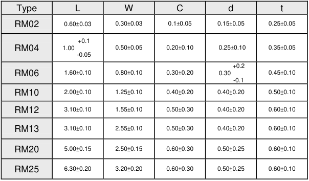
| 4. Dimensions: 0 UNIT: mm Type L W C d t RM02 0.60±0.03 0.30±0.03 0.1±0.05 0.15±0.05 0.25±0.05 +0.1 RM04 1.00 0.50±0.05 0.20±0.10 0.25±0.10 0.35±0.05 -0.05 +0.2 RM06 1.60±0.10 0.80±0.10 0.30±0.20 0.30 0.45±0.10 -0.1 RM10 2.00±0.10 1.25±0.10 0.40±0.20 0.40±0.20 0.50±0.10 RM12 3.10±0.10 1.55±0.10 0.50±0.30 0.40±0.20 0.60±0.10 RM13 3.10±0.10 2.55±0.10 0.50±0.30 0.40±0.20 0.60±0.10 RM20 5.00±0.15 2.50±0.15 0.60±0.30 0.50±0.25 0.60±0.10 RM25 6.30±0.20 3.20±0.20 0.60±0.30 0.50±0.25 0.60±0.10 | |||
Page 3
| TA-I | Thick Film Chip Resistors ( Lead – Free for RM 0 ohm series) | Document No. | TRM-XXOS102D |
| Revise Date | 2011/08/12 | ||
| page number | 3 /11 | ||
| 5. Ratings & Characteristics : OΩ THICK FILM CHIP RESISTORS DC DC inrush current (5 sec/one time) Type Rated Current Resistance Range Max Overload Current RM02 0.5A 1A 50mΩ MAX RM04 1A 2.5A 50mΩ MAX RM06 1A 2.5A 50mΩ MAX RM10 2A 5A 50mΩ MAX RM12 2A 5A 50mΩ MAX RM13 2A 5A 50mΩ MAX RM20 2A 5A 50mΩ MAX RM25 2A 5A 50mΩ MAX Operating Temp(℃): : -55℃ 〜 +155℃ ( RM02 -55℃ 〜 +125℃ ) 5.1 Derating Curve : For resistors operated at ambient temperature over 70℃ , power rating shall be derated in accordance with figure 1. P max. 100 Power ratio ( % ) RM04/06/10 50 RM02 RM12/13/20/25 0 -55 50 70 100 125 155 Ambient Temp. ( C ) Figure 1 | |||
| OΩ THICK FILM CHIP RESISTORS | |||
| Type | Rated Current | DC DC inrush current (5 sec/one time) Max Overload Current | Resistance Range |
| RM02 | 0.5A | 1A | 50mΩ MAX |
| RM04 | 1A | 2.5A | 50mΩ MAX |
| RM06 | 1A | 2.5A | 50mΩ MAX |
| RM10 | 2A | 5A | 50mΩ MAX |
| RM12 | 2A | 5A | 50mΩ MAX |
| RM13 | 2A | 5A | 50mΩ MAX |
| RM20 | 2A | 5A | 50mΩ MAX |
| RM25 | 2A | 5A | 50mΩ MAX |
| Operating Temp(℃): : -55℃ 〜 +155℃ ( RM02 -55℃ 〜 +125℃ ) | |||
Page 4
| TA-I | Thick Film Chip Resistors ( Lead – Free for RM 0 ohm series) | Document No. | TRM-XXOS102D |
| Revise Date | 2011/08/12 | ||
| page number | 4 /11 | ||
| 6. Reliability Tests: Reference Test Items Condition of Test Test Limits standard Temperature Coefficient of IEC60115-1-4.8 -55〜 +125 ℃ Refer 5.0 Resistance JIS-C5201-4.8 IEC60115-1-4.13 2.5 X rated current for 5 sec Short Time Overload 0Ω : 50mΩ or less JIS-C5201-4.13 (Remarks : 0201 2.0 * RCWC) 2.5 X rated current EC60115-1-4.39 1sec “ON” ,25sec “OFF” , Intermittent Overload 0Ω : 50mΩ or less JIS-C5201-4.39 10000 cycles (Remarks : 0201 2.0 * RCWC) 1000 hours at rated voltage, 70 ℃ , IEC60115-1-4.25.1 Load Life 1.5hours 0Ω : 100mΩ or less JIS-C5201-4.25.1 “ON “, 0.5hour “OFF” IEC60115-1-4.24 1000 hours at rated voltage , 40±2℃, 0Ω : 100mΩ or less Load Life with Humidity JIS-C5201-4.24 90~95% RH 1.5hours “ON “, 0.5hour “OFF” Without mechanical damage Rapid Change of IEC60115-1-4.19 -55℃ (30 min. ) / +155 ℃(30 min. ) 0Ω : 50mΩ or less Temperature JIS-C5201-4.19 5 cycles At least 95% of surface area IEC60115-1-4.17 245±5℃ solder, 2±0.5 sec dwell. Solderability of electrode shall be covered JIS-C5201-4.17 Solder : Sn96.5 / Ag3.0 / Cu0.5 with new solder. Robustness of Termination IEC60115-1-4.33 3mm deflection (Bending) JIS-C5201-4.33 0Ω : 50mΩ or less Dielectric Withstanding IEC60115-1-4.7 Applying voltage : No abnormalities such as 0201 : 50V , 0402 & 0603 : 300V The flashover, burning dielectric Voltage (Voltage Proof) JIS-C5201-4.7 other 500V for a minute . breakdown shall appear. IEC60115-1-4.6 Applying voltage 100V for 1 minute. Insulation Resistance ≧1GΩ JIS-C5201-4.6 Remark : 0201 50V IEC60115-1-4.23.2 Resistance to Dry Heat 125±5℃ for 96±4Hrs 0Ω : 50mΩ or less JIS-C5201-4.23.2 IEC60115-1-4.18 Resistance to Solder Heat 270 ±5℃ solder , 10 ±1 sec dwell . 0Ω : 50mΩ or less JIS-C5201-4.18 Note* : RCWC : Rated continuous working current . 7. Marking 7.1 1 digit, e.g.,:(E-24) 0 = 0Ω. 7.2 No Marking for RM02 & RM04 | |||
| Test Items | Reference standard | Condition of Test | Test Limits |
|---|---|---|---|
| Temperature Coefficient of Resistance | IEC60115-1-4.8 JIS-C5201-4.8 | -55〜 +125 ℃ | Refer 5.0 |
| Short Time Overload | IEC60115-1-4.13 JIS-C5201-4.13 | 2.5 X rated current for 5 sec (Remarks : 0201 2.0 * RCWC) | 0Ω : 50mΩ or less |
| Intermittent Overload | EC60115-1-4.39 JIS-C5201-4.39 | 2.5 X rated current 1sec “ON” ,25sec “OFF” , 10000 cycles (Remarks : 0201 2.0 * RCWC) | 0Ω : 50mΩ or less |
| Load Life | IEC60115-1-4.25.1 JIS-C5201-4.25.1 | 1000 hours at rated voltage, 70 ℃ , 1.5hours “ON “, 0.5hour “OFF” | 0Ω : 100mΩ or less |
| Load Life with Humidity | IEC60115-1-4.24 JIS-C5201-4.24 | 1000 hours at rated voltage , 40±2℃, 90~95% RH 1.5hours “ON “, 0.5hour “OFF” | 0Ω : 100mΩ or less Without mechanical damage |
| Rapid Change of Temperature | IEC60115-1-4.19 JIS-C5201-4.19 | -55℃ (30 min. ) / +155 ℃(30 min. ) 5 cycles | 0Ω : 50mΩ or less |
| Solderability | IEC60115-1-4.17 JIS-C5201-4.17 | 245±5℃ solder, 2±0.5 sec dwell. Solder : Sn96.5 / Ag3.0 / Cu0.5 | At least 95% of surface area of electrode shall be covered with new solder. |
| Robustness of Termination (Bending) | IEC60115-1-4.33 JIS-C5201-4.33 | 3mm deflection | 0Ω : 50mΩ or less |
| Dielectric Withstanding Voltage (Voltage Proof) | IEC60115-1-4.7 JIS-C5201-4.7 | Applying voltage : 0201 : 50V , 0402 & 0603 : 300V The other 500V for a minute . | No abnormalities such as flashover, burning dielectric breakdown shall appear. |
| Insulation Resistance | IEC60115-1-4.6 JIS-C5201-4.6 | Applying voltage 100V for 1 minute. Remark : 0201 50V | ≧1GΩ |
| Resistance to Dry Heat | IEC60115-1-4.23.2 JIS-C5201-4.23.2 | 125±5℃ for 96±4Hrs | 0Ω : 50mΩ or less |
| Resistance to Solder Heat | IEC60115-1-4.18 JIS-C5201-4.18 | 270 ±5℃ solder , 10 ±1 sec dwell . | 0Ω : 50mΩ or less |
Page 5
| TA-I | Thick Film Chip Resistors ( Lead – Free for RM 0 ohm series) | Document No. | TRM-XXOS102D |
| Revise Date | 2011/08/12 | ||
| page number | 5 /11 | ||
| 8. Taping & Reel : 8.1 Taping Dimensions 8.1.1 4 mm pitch paper: Packing Type A B W F E P P P D T 1 2 0 0 RM06 1.1±0.1 1.9±0.1 0.64±0.1 RM10 1.6±0.15 2.4±0.2 +0.1 Paper RM12 2.0±0.15 3.6±0.2 8.0±0.2 3.5±0.05 1.75±0.1 4.0±0.1 2.0±0.05 4.0±0.1 ψ1.5 0.84±0.1 RM13 2.8±0.2 3.6±0.2 -0 8.1.2 2 mm pitch paper : Packing Type A B W F E P P P D T 1 2 0 0 RM02 0.37±0.05 0.67±0.1 2.0±0.1 2.0±0.05 0.37±0.1 Paper RM04 0.7±0.05 1.2±0.05 2.0±0.1 2.0±0.1 4.0±0.1 +0.1 0.45±0.1 8.0±0.2 3.5±0.05 1.75±0.1 ψ1.5 RM06 1.1±0.1 1.9±0.1 2.0±0.1 2.0±0.1 -0 0.64±0.1 | |||
| Packing | Type | A | B | W | F | E | P 1 | P 2 | P 0 | D 0 | T |
|---|---|---|---|---|---|---|---|---|---|---|---|
| Paper | RM06 | 1.1±0.1 | 1.9±0.1 | 8.0±0.2 | 3.5±0.05 | 1.75±0.1 | 4.0±0.1 | 2.0±0.05 | 4.0±0.1 | +0.1 ψ1.5 -0 | 0.64±0.1 |
| RM10 | 1.6±0.15 | 2.4±0.2 | 0.84±0.1 | ||||||||
| RM12 | 2.0±0.15 | 3.6±0.2 | |||||||||
| RM13 | 2.8±0.2 | 3.6±0.2 |
| Packing | Type | A | B | W | F | E | P 1 | P 2 | P 0 | D 0 | T |
|---|---|---|---|---|---|---|---|---|---|---|---|
| Paper | RM02 | 0.37±0.05 | 0.67±0.1 | 8.0±0.2 | 3.5±0.05 | 1.75±0.1 | 2.0±0.1 | 2.0±0.05 | 4.0±0.1 | +0.1 ψ1.5 -0 | 0.37±0.1 |
| RM04 | 0.7±0.05 | 1.2±0.05 | 2.0±0.1 | 2.0±0.1 | 0.45±0.1 | ||||||
| RM06 | 1.1±0.1 | 1.9±0.1 | 2.0±0.1 | 2.0±0.1 | 0.64±0.1 |
Page 6
| TA-I | Thick Film Chip Resistors ( Lead – Free for RM 0 ohm series) | Document No. | TRM-XXOS102D |
| Revise Date | 2011/08/12 | ||
| page number | 6 /11 | ||
| 8.1.3 4 mm pitch Emboss : Packing Type A B W F E P P P D T 1 2 0 0 RM20 2.8±0.2 5.3±0.2 +0.1 Emboss 12.0±0.2 5.5±0.05 1.75±0.1 4.0±0.1 2.0±0.05 4.0±0.05 ψ1.5 0.85±0.15 RM25 3.6±0.2 6.9±0.2 -0 8.2 Reel Specifications : UNIT: mm Type ψA ψB ψC W T RM02 /04 / 06 9.0 ± 1.0 11.5 ± 1.0 RM10 /12 /13 178.0 ± 2.0 60.0 ± 1.0 13.0 ± 1.0 RM20 / 25 13.0 ± 1.0 15.5 ± 1.0 | |||
| Packing | Type | A | B | W | F | E | P 1 | P 2 | P 0 | D 0 | T |
|---|---|---|---|---|---|---|---|---|---|---|---|
| Emboss | RM20 | 2.8±0.2 | 5.3±0.2 | 12.0±0.2 | 5.5±0.05 | 1.75±0.1 | 4.0±0.1 | 2.0±0.05 | 4.0±0.05 | +0.1 ψ1.5 -0 | 0.85±0.15 |
| RM25 | 3.6±0.2 | 6.9±0.2 |
| Type | ψA | ψB | ψC | W | T |
|---|---|---|---|---|---|
| RM02 /04 / 06 RM10 /12 /13 | 178.0 ± 2.0 | 60.0 ± 1.0 | 13.0 ± 1.0 | 9.0 ± 1.0 | 11.5 ± 1.0 |
| RM20 / 25 | 13.0 ± 1.0 | 15.5 ± 1.0 |
Page 7
| TA-I | Thick Film Chip Resistors ( Lead – Free for RM 0 ohm series) | Document No. | TRM-XXOS102D |
| Revise Date | 2011/08/12 | ||
| page number | 7 /11 | ||
| 8.3. Peel –off force : Peel –off force of paper and blister tape is in accordance with “JIS-C5202 ” that is , 0.1 to 0.7 N at a peel-off speed of 300 mm / minute. pull top cover tape 300 mm/min 10〜15∘ standard: 0.1 ~ 0.7 N carrier tape 9. Label : 9.1 Manufacture Label : Date Code Resistance Tolerance Type QTY: 5000 PCS 0 J Lot No: 00860166K- 0008 0603 | |||
Page 8
| TA-I | Thick Film Chip Resistors ( Lead – Free for RM 0 ohm series) | Document No. | TRM-XXOS102D |
| Revise Date | 2011/08/12 | ||
| page number | 8 /11 | ||
| Customer Label ( By customer request ): Lead-Free Products TA-I TECH LEAD FREE 0603 5%(T) 0Ω Product Spec. 105A702723 RM06JTN0 Customer No: 0 4 .0 5 . 2 1 Date Year Month 10. Recommended land patterns : Land pattern Dimension ( mm ) a b c Type Size RM 02 (0201 ) 0.25~0.3 0.7~0.9 0.3~0.4 RM 04 (0402 ) 0.50~0.6 1.4~1.6 0.4~0.6 RM 06 (0603 ) 0.7~0.9 2.0~2.2 0.8~1.0 RM 10 (0805 ) 1.0~1.4 3.2~3.8 0.9~1.4 RM 12 (1206 ) 2.0~2.4 4.4~5.0 1.2~1.8 RM 13 (1210 ) 2.0~2.4 4.4~5.0 2.3~3.5 RM 20 (2010 ) 3.3~3.7 5.7~6.5 2.3~3.5 RM 25 (2512 ) 3.6~4.0 7.6~8.6 2.3~3.5 | |||
| Land pattern Type Size | Dimension ( mm ) | |||
|---|---|---|---|---|
| a | b | c | ||
| RM | 02 (0201 ) | 0.25~0.3 | 0.7~0.9 | 0.3~0.4 |
| RM | 04 (0402 ) | 0.50~0.6 | 1.4~1.6 | 0.4~0.6 |
| RM | 06 (0603 ) | 0.7~0.9 | 2.0~2.2 | 0.8~1.0 |
| RM | 10 (0805 ) | 1.0~1.4 | 3.2~3.8 | 0.9~1.4 |
| RM | 12 (1206 ) | 2.0~2.4 | 4.4~5.0 | 1.2~1.8 |
| RM | 13 (1210 ) | 2.0~2.4 | 4.4~5.0 | 2.3~3.5 |
| RM | 20 (2010 ) | 3.3~3.7 | 5.7~6.5 | 2.3~3.5 |
| RM | 25 (2512 ) | 3.6~4.0 | 7.6~8.6 | 2.3~3.5 |
Page 9
| TA-I | Thick Film Chip Resistors ( Lead – Free for RM 0 ohm series) | Document No. | TRM-XXOS102D |
| Revise Date | 2011/08/12 | ||
| page number | 9 /11 | ||
| 11. Recommend IR – Reflow profile : (solder : Sn96.5 / Ag3 / Cu0.5) 5 Peak : 250 ℃ , 5 sec 0 Pre – heat Zone : 150 to 180 ℃, 90±30 sec Soldering Zone : 230℃ or higher , 30±10 sec 12. Storage Conditions: Temperature: 5℃~35℃,Humidity:40%~75% 13. Shelf Life: 2 years from manufacturing date. 14. ECN : Engineering Change Notice: The customer will be informed with ECN if there is significant modification on the characteristics and materials described in Approval Sheet. | |||
Page 10
| TA-I | Thick Film Chip Resistors ( Lead – Free for RM 0 ohm series) | Document No. | TRM-XXOS102D |
| Revise Date | 2011/08/12 | ||
| page number | 10 /11 | ||
| 15. Manufacturing Country & City : TA-I TECHNOLOGY CO., LTD. ( Taiwan– Tao Yuan ) Tel: 886-3-3246169 Fax : 886-3-3246167 Associated companies : (1) FORTUNE TASK RESISTOR FACTORY ( China – Dongguan ) Tel : 86-769-8339-4790〜3 Fax : 86-769-8339-4794 (2) TA-I TECHNOLOGY (DONGGUAN ) CO., LTD. ( China –Dongguan ) Tel : 86-769-8339-4790〜3 Fax : 86-769-8339-4794 (3) TA-I TECHNOLOGY ( SU ZHOU ) CO., LTD. ( China – Su Zhou) Tel :86- 512-63457879 Fax : 86-512-63457869 (4) TAI OHM ELECTRONICS ( M ) SDN. BHD. ( Malaysia – Pulaupinang ) Tel :604- 3900480 Fax : 604-3901481 (5) P.T.TAI ELECTRONICS Indonesia ( Indonesia – Jakarta ) Tel :002-62-21-44820254 Fax : 002-62-21-44820256 | |||
Page 11
| TA-I | Thick Film Chip Resistors ( Lead – Free for RM 0 ohm series) | Document No. | TRM-XXOS102D |
| Revise Date | 2011/08/12 | ||
| page number | 11 /11 | ||
| Revise record Date Content Owner 6. Reliability Tests: (As specified in JIS C 5202) Short Time Overload & Intermittent Overload Apr. 19. 2007 Vincent Voltage change to current Reliability test : March.01.2011 Reference standard from JIS-5202 change to IEC60115 & Kate JIS-C5201 Operating Temp(℃): From -55℃ 〜 +125℃ June 24.2011 change to -55℃ 〜 +155℃ ( RM02 -55℃ 〜 +125℃ ) kate | |||
| Date | Content | Owner |
| Apr. 19. 2007 | 6. Reliability Tests: (As specified in JIS C 5202) Short Time Overload & Intermittent Overload Voltage change to current | Vincent |
| March.01.2011 | Reliability test : Reference standard from JIS-5202 change to IEC60115 & JIS-C5201 | Kate |
| June 24.2011 | Operating Temp(℃): From -55℃ 〜 +125℃ change to -55℃ 〜 +155℃ ( RM02 -55℃ 〜 +125℃ ) | kate |