


 Download PDF
RM008 SKYWORKS
Document overview
- PDF pages: 12
Technical content
Page 1
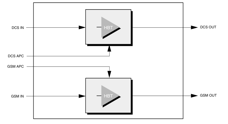
The RM008 is a dual-band Power Amplifier Module (PAM) designed in a compact form factor for Class 4 GSM900 and Class 1 DCS1800 operation. The PAM consists of two Gallium Arsenide (GaAs) Heterojunction Bipolar Transistor (HBT) power amplifiers and internal components that match the RF input and output ports to 50 ohms, which reduces the number of external components for a dual-band design. Optimized for lithium-ion battery operation, both PAs share common power supply pins to distribute current. The RM008 dual PAM has extremely low standby current, which maximizes handset standby time. A block diagram of the RM008 is shown below. The Analog Power Control (APC) pins
(GSM APC and DCS APC), control output power level. Table 4 of this data sheet shows the complete signal pin assignments and descriptions of the RM008 dual-band Power Amplifier Module.
Functional Block Diagram
Distinguishing Features
- High efficiency GSM 50% DCS 45%
- Input and output matching 50 ohms internal
- Small outline 9.1 mm x 11.61 mm
- Low profile 1.64 mm
Applications
- Class 4 GSM900 and Class 1 DCS1800 dual-band cellular handsets
Data Sheet © 1999–2002 Skyworks Solutions, Inc., All Rights Reserved.
Page 2
Electrical Characteristics
Electrical Characteristics
The following tables list the electrical characteristics of the RM008 Power Amplifier. Table 1 depicts the absolute maximum ratings and Table 2 specifies the recommended operating conditions
to achieve the performance specifications in Table 3.
Table 1. Absolute Maximum Ratings
| Parameter | Minimum | Maximum | Units |
|---|---|---|---|
| Supply Voltage (VCC) | — | 7 | V |
| Storage Temperature | –55 | +125 | °C |
Table 2. Recommended Operating Conditions
| Parameter | Minimum | Typical | Maximum | Units |
|---|---|---|---|---|
| Supply Voltage (VCC) | 2.9 | 3.3 | 4.6 | V |
| Temperature | –30 | — | +85 | °C |
Table 3. Electrical Specifications for Nominal Operating Conditions (1 of 2)
| Parameter | Test Conditions | Symbol | Minimum | Typical | Maximum | Units |
|---|---|---|---|---|---|---|
| GSM Mode (f = 880–915 MHz and P = 8 to 13 dBm) IN | ||||||
| Frequency Range | — | f1 | 880 | — | 915 | MHz |
| Input Power | — | PINGSM | 8 | 10 | 13 | dBm |
| Control Voltage Range | VGSMAPC | VAPC | 0.2 | — | 2.5 | V |
| Control Current Into VAPC | — | l GSMAPC | — | 40 | 70 | mA |
| Leakage Current | VCC = 4.6 V VAPC = 0 V | I LEAKAGE | — | — | 25 | µA |
| Efficiency | PINGSM = 10 dBm POUTGSM = 34 dBm | η GSM | — | 50 | — | % |
| 2nd Harmonic Distortion | POUTGSM = 34.5 dBm | H 2GSM | — | — | –5 | dBm |
| 3rd–7th Harmonic Distortion | POUTGSM = 34.5 dBm | H3–H7 | — | — | –7 | dBm |
| Output Power | PINGSM = 10 dBm | POUTGSM | 34.0 | 34.5 | — | dBm |
| PINGSM = 10 dBm VCC = 2.9 V TCASE = –30 °C to +85 °C | POUTDCS | 32.5 | 33.0 | — | dBm | |
| Input VSWR | All | VSWR (IN) | — | 1.5:1 | 2:1 | — |
Page 3
Electrical Characteristics
Table 3. Electrical Specifications for Nominal Operating Conditions (2 of 2)
| Parameter | Test Conditions | Symbol | Minimum | Typical | Maximum | Units |
|---|---|---|---|---|---|---|
| Isolation | PINGSM = 10 dBm APC = 0.5 V | — | — | — | –30 | dBm |
| Stability Condition VSWR(load) (no spurious oscillation > –35 dBm) | — | — | — | — | 8:1 all angles | — |
| Load Mismatch VSWR(load) (no damage/degradation) | — | — | — | — | 10:1 all angles | — |
| Noise Floor | PINGSM = 10 dBm BW = 100 kHz fO ±20 MHz offset | — | — | — | –85 | dBm |
| Full Power Control Voltage | POUTGSM = 34.5 dBm | — | — | 2.0 | — | — |
| DCS Mode (f = 1710–1785 MHz and P = 6 to 11 dBm) IN | ||||||
| Frequency Range | — | f2 | 1710 | — | 1785 | MHz |
| Input Power | — | PINDCS | 6 | 8.0 | 11 | dBm |
| Control Voltage Range | VDCSAPC | VAPC | 0.2 | — | 2.5 | V |
| Control Current Into VAPC | — | l DCSAPC | — | 30 | 70 | mA |
| Leakage Current | VCC = 4.6 V VAPC = 0 V | I LEAKAGE | — | — | 25 | µA |
| Efficiency | PINDCS = 8 dBm POUTDCS = 32 dBm | η DCS | — | 45 | — | % |
| 2nd Harmonic Distortion | POUTDCS = 32.5 dBm | H 2DCS | — | — | –7 | dBm |
| 3rd–7th Harmonic Distortion | POUTDCS = 32.5 dBm | H3–H7 | — | — | –7 | dBm |
| Output Power | PINDCS = 8 dBm | POUTDCS | 32.0 | 32.5 | — | dBm |
| PINDCS = 8 dBm VCC = 2.9 V TCASE = –30 °C to +85 °C | POUTDCS | 30.5 | 31.0 | — | dBm | |
| Input VSWR | All | VSWR (IN) | — | 1.5:1 | 2:1 | — |
| Isolation | PINDCS = 8 dBm APC = 0.5 V | — | — | — | –35 | dBm |
| Stability Condition VSWR (load) no spurious oscillation > –35 dBm) | — | — | — | — | 8:1 all angles | — |
| Load Mismatch VSWR(load) (no damage/degradation) | — | — | — | — | 10:1 all angles | — |
| Noise Floor DCS1800 | PINDCS = 8 dBm BW = 100 kHz fO ±20 MHz offset | — | — | — | –77 | dBm |
| Full Power Control Voltage | POUTDCS = 32.5 dBm | — | — | 2.0 | — | — |
| NOTE(S): TCASE = 25 °C, RL = 50Ω, pulsed operation with pulse width = 577 µsec and duty cycle of 1:8, VCC = 3.3 V unless specified otherwise | ||||||
Page 4
Electrical Characteristics
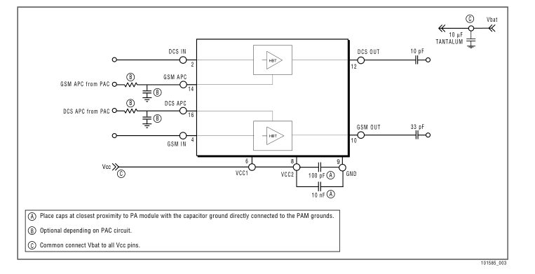
Figure 1. Typical RM008 PAM Application
Page 5
Package Dimensions and Pin Descriptions
Package Dimensions and Pin Descriptions
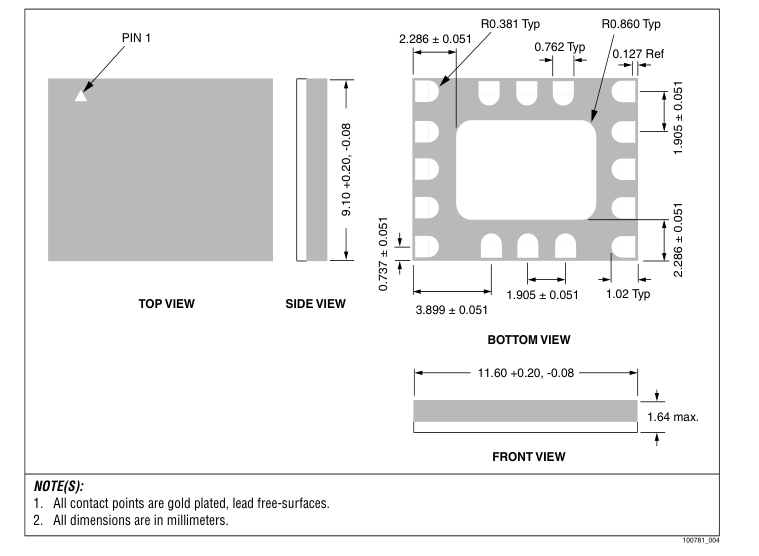
Figure 2 provides the package dimensions for the 16-pin RM008 leadless MCM. Figure 3 shows the device pin configuration and Table 4 lists the pins and signal descriptions.
Figure 2. RM008 Package Dimensions—16-pin PAM (All Views)
Page 6
Package Dimensions and Pin Descriptions
Figure 3. RM008 Pin Configuration–16-Pin Leadless PAM (Top View)
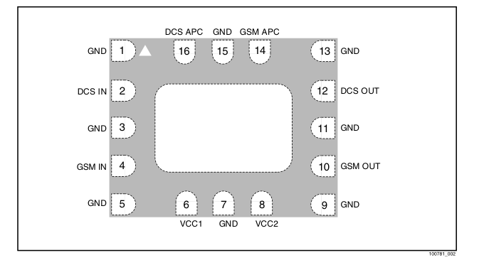
Table 4. RM008 Pin and Signal Descriptions
| PIN | NAME | DESCRIPTION | PIN | NAME | DESCRIPTION |
|---|---|---|---|---|---|
| 1 | GND | Ground | 9 | GND | Ground |
| 2 | DCS IN | RF input to DCS PA | 10 | GSM OUT | GSM RF output (DC coupled) |
| 3 | GND | Ground | 11 | GND | Ground |
| 4 | GSM IN | RF input to GSM PA | 12 | DCS OUT | DCS RF output (DC coupled) |
| 5 | GND | Ground | 13 | GND | Ground |
| 6 | VCC2 | Power supply for PA driver stages | 14 | GSM APC | GSM analog power control |
| 7 | GND | Ground | 15 | GND | Ground |
| 8 | VCC2 | Power supply for PA output stages | 16 | DCS APC | DCS analog power control |
Page 7
Package and Handling Information
Package and Handling Information
Because of its sensitivity to moisture absorption, this device package is baked and vacuum packed prior to shipment. Instructions on the shipping container label must be followed regarding exposure to moisture after the container seal is broken, otherwise, problems related to moisture absorption may occur when the part is subjected to high temperature during solder assembly.
The RM008 is capable of withstanding an MSL 3/240 °C solder reflow. Care must be taken when attaching this product, whether it is done manually or in a production solder reflow environment. If the part is attached in a reflow oven, the temperature ramp rate should not exceed 5 °C per second; maximum temperature should not exceed 240 °C. If the part is manually attached, precaution should be taken to insure that the part is not subjected to temperatures exceeding 240 °C for more than 10 seconds.
For details on both attachment techniques, precautions, and handling procedures recommended by Skyworks, please refer to Application Note: PCB Design and SMT Assembly/Rework, Document Number 101752. Additional information on standard SMT reflow profiles can also be found in the JEDEC Standard J–STD–020A.
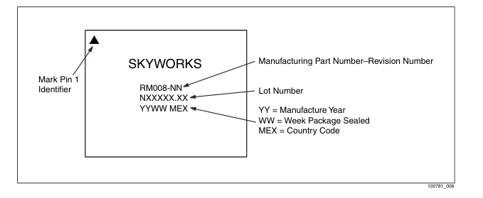
Figure 4. Typical Case Markings
Page 8
Package and Handling Information
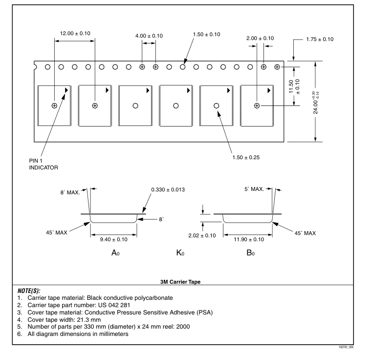
Production quantities of this product are shipped in the standard tape and reel format illustrated in Figure 5.
Figure 5. RM008 Tape and Reel – 9.1 mm x 11.6 mm
Page 9
Electrostatic Discharge Sensitivity
Electrostatic Discharge Sensitivity
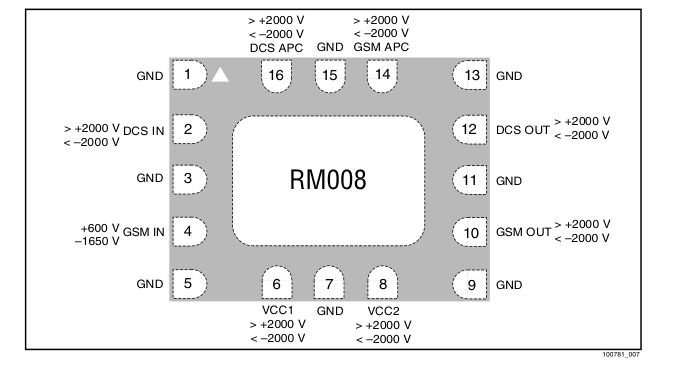
The RM008 is a Class I device. Figure 6 lists the Electrostatic Discharge (ESD) immunity level for each pin of the RM008 product. The numbers in Figure 6 specify the ESD threshold level for each
pin where the I-V curve between the pin and ground starts to show degradation. The ESD testing was performed in compliance with MIL-STD-883E Method 3015.7 using the Human Body Model.
Since 2000 volts represents the maximum measurement limit of the test equipment used, pins marked > 2000 V pass 2000V ESD stress.
Figure 6. ESD Sensitivity Ares (Top View)
Various failure criteria can be utilized when performing ESD testing. Many vendors employ relaxed ESD failure standards which fail devices only after “the pin fails the electrical specification
limits” or “the pin becomes completely non-functional”. Skyworks employs most stringent criteria, fails devices as soon as the pin begins to show any degradation on a curve tracer.
To avoid ESD damage, both latent and visible, it is very important that the product assembly and test areas follow the Class-1 ESD handling precautions listed in Table 5.
Table 5. Precautions for GaAs ICs with ESD Thresholds Greater Than 200 V But Less Than 2000 V
| Personnel Grounding Wrist Straps Conductive Smocks, Gloves and Finger Cots Antistatic ID Badges | Facility Relative Humidity Control and Air Ionizers Dissipative Floors (less than 109 Ω to GND) |
| Protective Workstation Dissipative Table Tops Protective Test Equipment (Properly Grounded) Grounded Tip Soldering Irons Conductive Solder Suckers Static Sensors | Protective Packaging & Transportation Bags and Pouches (Faraday Shield) Protective Tote Boxes (Conductive Static Shielding) Protective Trays Grounded Carts Protective Work Order Holders |
Page 10
Electrostatic Discharge Sensitivity
Page 11
Ordering Information
| Model Number | Manufacturing Part Number | Product Revision | Package | Operating Temperature |
|---|---|---|---|---|
| RM008 | RM008–23 | 23 | –30 °C to +85 °C |
Revision History
| Revision | Level | Date | Description |
|---|---|---|---|
| A | October 1999 | Initial Release | |
| B | October 2000 | Revise: Table 4; Figure 4 | |
| C | May 2001 | Revise: Converted to standard format; Figure 1 Add: ESD data; Packaging and Handling Information | |
| D | July 26, 2002 | Revise: Part Number to RM008–23; ESD data, Package and Handling Add: New Figure 5 |
References
Application Note: PCB Design and SMT Assembly/Rework, Document Number 101752
JEDEC Standard J–STD–020A.
© 1999–2002, Skyworks Solutions, Inc. All Rights Reserved.
Information in this document is provided in connection with Skyworks Solutions, Inc. ("Skyworks") products. These materials are provided by Skyworks as a service to its customers and may be used for informational purposes only. Skyworks assumes no responsibility for errors or omissions in these materials. Skyworks may make changes to its products, specifications and product descriptions at any time, without notice. Skyworks makes no commitment to update the information and shall have no responsibility whatsoever for conflicts, incompatibilities, or other difficulties arising from future changes to its products and product descriptions.
No license, express or implied, by estoppel or otherwise, to any intellectual property rights is granted by this document. Except as may be provided in Skyworks' Terms and Conditions of Sale for such products, Skyworks assumes no liability whatsoever.
THESE MATERIALS ARE PROVIDED "AS IS" WITHOUT WARRANTY OF ANY KIND, EITHER EXPRESS OR IMPLIED, RELATING TO SALE AND/OR USE OF SKYWORKS™ PRODUCTS INCLUDING WARRANTIES RELATING TO FITNESS FOR A PARTICULAR PURPOSE, MERCHANTABILITY, PERFORMANCE, QUALITY OR NON-INFRINGEMENT OF ANY PATENT, COPYRIGHT OR OTHER INTELLECTUAL PROPERTY RIGHT. SKYWORKS FURTHER DOES NOT WARRANT THE ACCURACY OR COMPLETENESS OF THE INFORMATION, TEXT, GRAPHICS OR OTHER ITEMS CONTAINED WITHIN THESE MATERIALS. SKYWORKS SHALL NOT BE LIABLE FOR ANY SPECIAL, INDIRECT, INCIDENTAL, OR CONSEQUENTIAL DAMAGES, INCLUDING WITHOUT LIMITATION, LOST REVENUES OR LOST PROFITS THAT MAY RESULT FROM THE USE OF THESE
MATERIALS.
Skyworks™ products are not intended for use in medical, lifesaving or life-sustaining applications. Skyworks' customers using or selling Skyworks™ products for use in such applications do so at their own risk and agree to fully indemnify Skyworks for any damages resulting from such improper use or sale.
The following are trademarks of Skyworks Solutions, Inc.: Skyworks™, the Skyworks symbol, and "Breakthrough Simplicity"™. Product names or services listed in this publication are for identification purposes only, and may be trademarks of third parties. Thirdparty brands and names are the property of their respective owners.
Additional information, posted at www.skyworksinc.com, is incorporated by reference.
Page 12

General Information: Skyworks Solutions, Inc. 4311 Jamboree Rd. Newport Beach, CA. 92660-3007 www.skyworksinc.com