


 Download PDF
877049 YAGEO
Document overview
- PDF pages: 9
Technical content
Page 1
Page 2

ORDERING INFORMATION - GLOBAL PART NUMBER & 12NC
SCOPE
Both part numbers are identified by the series, size, tolerance, packing
This specification describes
type, temperature coefficient, taping reel and resistance value.
RL0402 to RL2512 low ohmic chip resistors with lead-free terminations
D oorrddeerriinngg ccooddee
YYA AG
GEEO
O BBRRA
AN ND
made by thick film process.
GLOBAL PART NUMBER (PREFERRED)
RL XXXX X X X XX XXXX L
APPLICATIONS
(1) (2) (3) (4) (5) (6) (7)
z Converters
(1) SIZE
z Printer equipment
0402 / 0603 / 0805 / 1206 / 1210 / 1218 / 2010 / 2512
z Server board z Telecom
(2) TOLERANCE
z Consumer
F = ±1% G = ±2%
FEATURES
J = ±5%
z Halogen Free Epoxy
(3) PACKAGING TYPE
z RoHS compliant
R = Paper taping reel
K = Embossed taping reel
- Products with lead free
(4) TEMPERATURE COEFFICIENT OF RESISTANCE
terminations meet RoHS requirements
– = Base on spec
- Pb-glass contained in electrodes,
(5) TAPING REEL
resistor element and glass are exempted by RoHS
10 = 10 inch dia. Reel 13 = 13 inch dia. Reel
07 = 7 inch dia. Reel
z Reducing environmentally
(6) RESISTANCE VALUE
hazardous wastes
There are 2~4 digits indicated the resistor value. Letter R/K/M is decimal point, no need
z High component and equipment
to mention the last zero after R/K/M, e.g.1K2, not 1K20.
reliability
Detailed resistance rules show in table of “Resistance rule of global part number”.
z Saving of PCB space z None forbidden-materials used
(7) DEFAULT CODE
in products/production
Letter L is system default code for order only (Note)
z Low resistances applied to
Letter H is Halogen / Lead free (special code on request)
current sensing
Resistance rule of global part number Resistance code rule
0RXXX (1 to 976 mΩ)
XRXX (1 to 9.76 Ω)
XXRX (10 to 97.6 Ω) XXXR (100 to 976 Ω) XKXX (1 to 9.76 KΩ) XMXX
ORDERING EXAMPLE
The ordering code of a RL0603
Example
chip resistor, value 0.56 X with ±1% tolerance, supplied in 7-inch
0R1 = 0.1 Ω
tape reel is: RL0603FR-070R56L.
0R12 = 0.12 Ω 0R105 = 0.105 Ω
NOTE
1R = 1 Ω
- All our RSMD products meet RoHS
1R5 = 1.5 Ω
compliant and Halogen Free. "LFP" of
9R76 = 9.76 Ω
the internal 2D reel label mentions
10R = 10 Ω
"Lead Free Process"
97R6 = 97.6 Ω
- On customized label, "LFP" or specific symbol can be printed
100R = 100 Ω
1K = 1,000 Ω 9K76 = 9760 Ω 1M = 1,000,000 Ω
(1 to 9.76 MΩ) 9M76= 9,760,000 Ω
Page 3

PPH
HYYC
CO OM
MPP BBRRA
AN ND D oorrddeerriinngg ccooddeess
Both GLOBAL PART NUMBER (preferred) and 12NC (traditional) codes are acceptable to order Phycomp brand products.
GLOBAL PART NUMBER (PREFERRED)
For detailed information of GLOBAL PART NUMBER and ordering example, please refer to page 2.
12NC CODE
2350 / 2390 / 2322 XXX XXXXX L
(1) (2) (3) (4)
EMBOSSED (2) PAPER/PE (2)
START TOL.RESISTANCE
TAPE ON REEL TAPE ON REEL (units)
SIZE TYPE
IN (1) (%) RANGE
4,000
5,000
10,000
0402 LRC31 2350 ±5% 0.05 to 1 Ω
-
- 513 20xxx
LRC32 2350 ±1% 0.05 to 1 Ω
-
- 513 22xxx
0603 LRC21 2350 ±5% 0.01 to 1 Ω
-
512 10xxx
-
LRC22 2350 ±1% 0.01 to 1 Ω
-
512 12xxx
-
0805 LRC11 2350 ±5% 0.01 to 1 Ω
-
511 10xxx
-
LRC12 2350 ±1% 0.01 to 1 Ω
-
511 12xxx
-
1206 LRC01 2350 ±5% 0.01 to 1 Ω
-
510 10xxx
-
LRC02 2350 ±1% 0.01 to 1 Ω
-
510 12xxx
-
1210 LPRC101 2390 ±5% 0.01 to 0.0976 Ω -
735 90xxx
-
LPRC101 2390 ±5% 0.1 to 1 Ω
-
735 60xxx
-
LPRC102 2390 ±1% 0.01 to 1 Ω
-
735 3xxxx
-
1218 LPRC201 2322 ±5% 0.01 to 1 Ω
735 64xxx
-
-
LPRC201 2322 ±1% 0.01 to 1 Ω
735 7xxxx
-
-
2010 LPRC111 2322 ±5% 0.01 to 0.0976 Ω 760 90xxx
-
-
LPRC111 2322 ±5% 0.1 to 1 Ω
760 60xxx
-
-
LPRC111 2322 ±1% 0.01 to 0.0976 Ω 761 90xxx
-
-
LPRC111 2322 ±1% 0.1 to 1 Ω
761 6xxxx
-
-
2512 LPRC221 2322 ±5% 0.01 to 0.0976 Ω 762 90xxx
-
-
LPRC221 2322 ±5% 0.1 to 1 Ω
762 60xxx
-
-
LPRC221 2322 ±1% 0.01 to 0.0976 Ω 763 90xxx
-
-
LPRC221 2322 ±1% 0.1 to 1 Ω
763 6xxxx
-
-
(1) The resistors have a 12-digit ordering code starting with 2350/2390/2322.
(2) The subsequent 4 or 5 digits indicate the resistor tolerance and packaging. (In 12NC code, only 07'' tape reel code is supplied. Supply of 10''/13'' tape reel is requested in Global part number ordering code.)
(3) The remaining 4 or 3 digits represent the resistance value with the last digit indicating the multiplier as shown in the table of “Last digit of 12NC”.
(4) Letter L is system default code for order only (Note). Letter H is Halogen / Lead free (special code on request).
Last digit of 12NC Resistance decade (3)
Last digit
0.01 to 0.0976 X
0
0.1 to 0.976 X
7
1 to 9.76 X
8
10 to 97.6 X 100 to 976 X
1
1 to 9.76 kX
2
10 to 97.6 kX
3
100 to 976 kX
4
1 to 9.76 MX
5
10 to 97.6 MX
6
Example: 0.02 X = 0200 or 200 0.3 X = 3007 or 307 1 X = 1008 or 108 33 kX = 3303 or 333 10 MX = 1006 or 106
ORDERING EXAMPLE
The ordering code of a RL0603 chip resistor, value 0.56 X with ±1% tolerance, supplied in tape of 5,000 units per reel is: 235051212567L or RL0603FR-070R56L.
NOTE
- All our RSMD products meet RoHS compliant and Halogen Free. "LFP" of the internal 2D reel label mentions "Lead Free Process" 2. On customized label, "LFP" or specific symbol can be printed
Page 4

MARKING RL0805 / RL1206 / RL1210 /RL1218 / RL2010 / RL2512
E-24 series / Non-series (R= 25/40/50/60/250/400/500 mΩ): 4 digits
020
The “R” is used as a decimal point; the other 3 digits are significant.
Fig. 1 Value = 20 mΩ
RL0603: R≥100 mX IN E-24 SERIES, R = 10/20/30/40/50/60 mΩ
3 digits
The “R” is used as a decimal point; the other 2 digits are significant.
Fig. 2 Value = 22 mΩ
RL0402 / RL0603: R<100 mX EXCEPT 10/20/30/40/50/60 mΩ
No marking
Fig. 3
For further marking information, please see special data sheet “Chip resistors marking”.
CONSTRUCTION The resistors are constructed out of a high-grade ceramic
OU
UTTLLIIN
NEESS
O
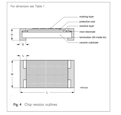
body. Internal metal electrodes are added at each end and connected by a resistive paste. The composition of the paste is adjusted to give the approximate required resistance and laser cutting of this resistive layer that achieves tolerance trims the value. The resistive layer is covered with a protective coat and printed with the resistance value. Finally, the two external terminations (matte tin) are added. See fig. 4.
DIMENSIONS Table 1 For outlines see fig. 4 TYPE L (mm) W (mm) H (mm) I1 (mm) I2 (mm) RL0402 1.00 ±0.10 0.50 ±0.05 0.35 ±0.05 0.20 ±0.10 0.25 ±0.10 RL0603 1.60 ±0.10 0.80 ±0.10 0.45 ±0.10 0.25 ±0.15 0.25 ±0.15 RL0805 2.00 ±0.10 1.25 ±0.10 0.50 ±0.10 0.35 ±0.20 0.35 ±0.20 RL1206 3.10 ±0.10 1.60 ±0.10 0.55 ±0.10 0.45 ±0.20 0.40 ±0.20 RL1210 3.10 ±0.10 2.60 ±0.15 0.55 ±0.10 0.50 ±0.20 0.50 ±0.20 RL1218 3.05 ±0.15 4.60 ±0.20 0.55 ±0.10 0.45 ±0.25 0.50 ±0.25 RL2010 5.00 ±0.10 2.50 ±0.15 0.55 ±0.10 0.60 ±0.20 0.50 ±0.20 RL2512 6.35 ±0.10 3.20 ±0.15 0.55 ±0.10 0.60 ±0.20 0.50 ±0.20
Page 5

ELECTRICAL CHARACTERISTICS Table 2
TEMPERATURE COEFFICIENT
TYPE / RESISTANCE RANGE
OF RESISTANCE
100mX≤R<500mX
500mX≤R<1X
RL0402 100mΩ≤R<1Ω
±800 ppm/°C
±300 ppm/°C
10mX≤R≤36mX
36mX<R≤91mX
91mX<R≤500mX
500mX<R<1X
RL0603 10mΩ≤R<1Ω
±1,500 ppm/°C
±1,200 ppm/°C
±800 ppm/°C
±300 ppm/°C
10mX≤R≤18mX 18mX<R≤47mX 47mX<R≤91mX 91mX<R≤360mX 360mX<R≤500mX 500mX<R<1X
RL0805
±1,500 ppm/°C ±1,200 ppm/°C ±1,000 ppm/°C
RL1206
±1,500 ppm/°C ±1,200 ppm/°C ±1,000 ppm/°C
10mΩ≤R<1Ω RL1210
±1,500 ppm/°C ±1,000 ppm/°C ±800 ppm/°C
RL2010
±1,500 ppm/°C ±1,200 ppm/°C ±1,000 ppm/°C
RL2512
±1,500 ppm/°C ±1,200 ppm/°C ±800 ppm/°C 10mX≤R≤30mX 30mX<R≤56mX
RL1218 10mΩ≤R<1Ω
±2,000 ppm/°C
±1,000 ppm/°C
FOOTPRINT AND SOLDERING PROFILES
±600 ppm/°C
±300 ppm/°C ±200 ppm/°C
±600 ppm/°C
±300 ppm/°C ±200 ppm/°C
±600 ppm/°C
±300 ppm/°C ±200 ppm/°C
±600 ppm/°C
±300 ppm/°C ±200 ppm/°C
±600 ppm/°C
±300 ppm/°C ±200 ppm/°C
56mX<R≤180mX
180mX<R<1X
±700 ppm/°C
±250 ppm/°C
For recommended footprint and soldering profiles, please see the special data sheet “Chip resistors mounting”.
PACKING STYLE AND PACKAGING QUANTITY Table 3 Packing style and packaging quantity PACKING STYLE
REEL DIMENSION RL0402 RL0603
Paper taping reel (R)
7" (178 mm) 10,000 5,000 10" (254 mm) 20,000 10,000 13" (330 mm) 50,000 20,000
Embossed taping reel (K)
7" (178 mm)
--- ---
NOTE
RL0805 RL1206 RL1210 RL1218 RL2010 RL2512
5,000 5,000 5,000
--- --- ---
10,000 10,000 10,000
--- --- ---
20,000 20,000 20,000
--- --- ---
--- --- --- 4,000 4,000
4,000
- For paper/embossed tape and reel specification/dimensions, please see the special data sheet “Chip resistors packing”.
Page 6

FUNCTIONAL DESCRIPTION
OPPEERRA
O ATTIIN
NG
GTTEEM
MPPEERRA
ATTU
URREE RRA
AN NG GEE
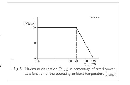
Range: –55 °C to +125 °C
PPO OW
WEERR RRA
ATTIIN
NG G
Each type rated power at 70 °C: RL0402=1/16 W; RL0603=1/10 W; RL0805=1/8 W; RL1206=1/4 W; RL1210=1/2 W; RL1218=1 W; RL2010=3/4 W; RL2512=1 W.
RATED VOLTAGE
The DC or AC (rms) continuous working voltage corresponding to the rated power is determined by the following formula:
V = √(P X R)
Where V = Continuous rated DC or AC (rms) working voltage (V) P = Rated power (W) R = Resistance value (X)
Page 7

TESTS AND REQUIREMENTS Table 4 Test condition, procedure and requirements
TEST
TEST METHOD
PROCEDURE
REQUIREMENTS
1,000 hours at 70±5 °C applied RCWV
IEC 60115-1 4.25.1
Life/
±2%
1.5 hours on, 0.5 hour off, still air required
Endurance
1,000 hours at maximum operating
IEC 60068-2-2
High Temperature
±1%
temperature depending on specification,
Exposure/ Endurance at upper
unpowered
category temperature
No direct impingement of forced air to the parts Tolerances: 125±5 °C
Each temperature / humidity cycle is defined at
MIL-STD-202G Method-106G
Moisture Resistance
±2%
8 hours (method 106F), 3 cycles / 24 hours for 10d with 25 °C / 65 °C 95% R.H, without steps 7a & 7b, unpowered Parts mounted on test-boards, without condensation on parts Measurement at 24±2 hours after test conclusion
MIL-STD-202G Method-107G
Thermal Shock
±1%
-55/+125 °C Note: Number of cycles required is 300. Devices unmounted Maximum transfer time is 20 seconds. Dwell time is 15 minutes. Air – Air
2.5 times RCWV or maximum overload
IEC60115-1 4.13
Short time overload
±2%
voltage whichever is less for 5 sec at room
No visible damage
temperature
Device mounted on PCB test board as
IEC 60068-2-21
Board Flex/
±1%
described, only 1 board bending required
Bending
No visible damage
3 mm bending Bending time: 60±5 seconds Ohmic value checked during bending
Page 8

TEST
TEST METHOD
PROCEDURE
REQUIREMENTS
Solderability
Electrical Test not required
IPC/JEDECJ-STD-002B test B
Well tinned (≥95% covered)
- Wetting
No visible damage
Magnification 50X SMD conditions: 1st step: method B, aging 4 hours at 155 °C dry heat 2nd step: leadfree solder bath at 245±3 °C Dipping time: 3±0.5 seconds
Leadfree solder, 260 °C, 30 seconds
IPC/JEDECJ-STD-002B test D
- Leaching
No visible damage
immersion time
Condition B, no pre-heat of samples.
IEC 60068-2-58
- Resistance to
±1%
Soldering Heat
Leadfree solder, 260 °C, 10 seconds
No visible damage
immersion time Procedure 2 for SMD: devices fluxed and cleaned with isopropanol
Page 9

REVISION HISTORY
CHANGE NOTIFICATION DESCRIPTION
REVISION DATE
Version 5 Mar 22, 2010 -
Version 4 Dec 11, 2008 -
Version 3 Aug 07, 2008 -
Version 2 Jul 15, 2005 -
Version 1 Apr 15, 2005 -
Version 0 Nov. 10, 2003 -
- The statement of "Halogen Free" on the cover added - Test methods updated
- Halogen Free Epoxy - Update global part number definition
- Change to dual brand datasheet that describe RL0402 to RL2512 with RoHS compliant
- Define global part number
- Ordering example revised
- Size 1218 extended
- Test method and procedure updated
- PE tape added (paper tape will be replaced by PE tape)
- First issue of this specification
“ Yageo reserves all the rights for revising the content of this datasheet without further notification, as long as the products itself are unchanged. Any product change will be announced by PCN.”