
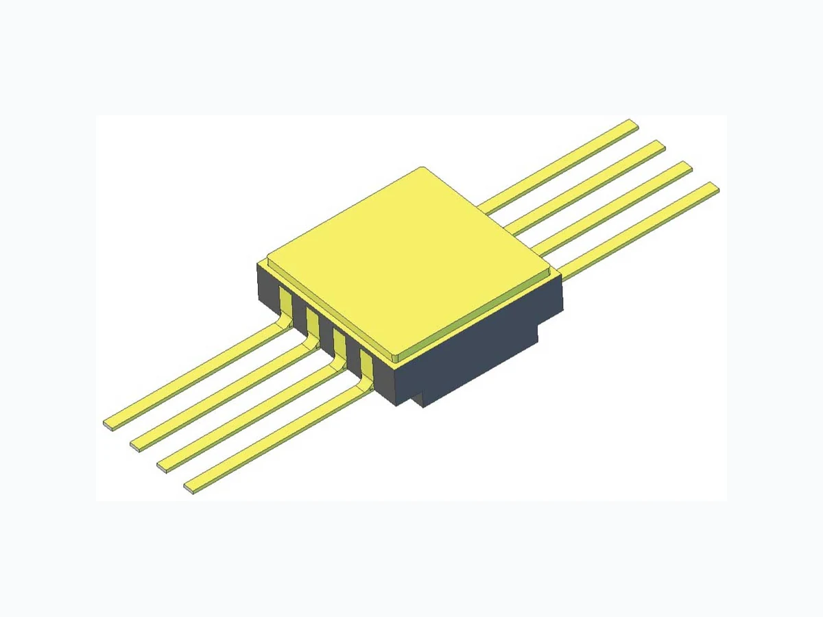
Datasheet - RHR801 - Rad-hard very high-speed comparator
Document overview
- Manufacturer or author: STMICROELECTRONICS
- PDF pages: 29
Technical content
Features
- Propagation time of 7 ns
- Rise/fall time: 1.1 ns on 10 pF
- Low consumption: 1.4 mA
- Single supply: 3 V to 5 V
- 100 krad high-dose rate
- No SEL at 120 MeV.cm²/mg
- SET characterized
- SMD pin : 5962R10215
- Mass : 0.45 g
Applications
- High-speed timing
- High-speed sampling
- Clock recovery
- Clock distribution
- Phase detectors
Description
The RHR801 is a very high-speed single comparator. It is designed to allow very high rise and fall times while drawing a high noise supply rejection. It uses a high-speed complementary BiCMOS process to achieve its very good speed/power ratio and its high tolerance to radiation. The RHR801 is mounted in a hermetic Flat-8 package. VDD VC C NC NC OUT NC IN - IN + The upper metallic lid is not electrically connected to any pins, nor to the IC die inside the package Ceramic Flat-8 Maturity status link RHR801 Rad-hard very high-speed comparator RHR801 Datasheet DS10316 - Rev 5 - April 2026 For further information, contact your local STMicroelectronics sales office.
1 Absolute maximum ratings and operating conditions
Table 1. Absolute maximum ratings
- VCC is defined as the voltage between the Vcc+ and Vcc- pins. The comparator can be used in single supply (for example,
Vcc+ = 5 V, Vcc- = 0 V) or dual supply (for example, Vcc+ = 2.5 V, Vcc- = -2.5 V).
- Differential voltages are the non-inverting input terminal with respect to the inverting input terminal. Vid should not exceed
- If the input voltage goes beyond the rails (above Vcc+ or below Vcc-), the ESD diodes may be activated. It is required in that
case to limit the input current to 10 mA with a serial resistor connected on the input.
- Short-circuits can cause excessive heating and destructive dissipation. Values are typical.
- Human body model: a 100 pF capacitor is charged to the specified voltage, then discharged through a 1.5 kΩ resistor
between two pins of the device. This is done for all couples of connected pin combinations while the other pins are floating.
- Machine model: a 200 pF capacitor is charged to the specified voltage, then discharged directly between two pins of the
while the other pins are floating.
- Charged device model: all pins and the package are charged together to the specified voltage and then discharged directly
to ground through only one pin. This is done for all pins. Table 2. Operating conditions
2 Electrical characteristics
Table 3. VCC+ = 3.3 V, VCC- = 0 V (unless otherwise specified)
Electrical characteristics
Symbol Parameter Test conditions Temp. Min. Typ. Max. Unit VOL Logic "0" voltage Isink = -3.3 mA 125°C 0 200 300 mV25°C 0 170 250 -55°C 0 150 200 Isink Output sink current Vout = VCC+ 125°C 14 17 20 mA 25°C 18 20 22 -55°C 19 22 26 Isource Output source current Vout = VCC- 125°C 17 20 23 25°C 20 22 25 -55°C 22 25 29 Power supply ICC-H High output supply current No load, VID = 0.1 V 125°C 1.40 1.55 2.10 mA 25°C 1.20 1.44 1.60 -55°C 0.95 1.13 1.30 ICC-L Low output supply current No load, VID = -0.1 V 125°C 1.60 1.75 2.3 25°C 1.30 1.63 1.80 -55°C 1.00 1.30 1.50 SVR Supply voltage rejection ratio (ΔVCC/ΔVio) VCC = 3 to 3.6 V, VICM = 1.65 V 125°C 42 65 dB 25°C 55 70 -55°C 45 65 CMRR Common-mode rejection ratio (ΔVic/ΔVio) VICM = 0.5 V to VCC -1.2 V 125°C 50 95 25°C 70 80 -55°C 60 85 RHR801
Table 4. VCC+ = 5 V, VCC- = 0 V (unless otherwise specified)
Symbol Parameter Test conditions Temp. Min. Typ. Max. Unit Isink Output sink current Vout = VCC+ 125°C 25 30 35 mA 25°C 30 35 40 -55°C 30 40 45 Isource Output source current Vout = VCC- 125°C 35 40 45 25°C 40 45 50 -55°C 45 50 55 Power supply ICC-H High output supply current No load, VID = 0.1 V 125°C 1.50 1.84 2.30 mA 25°C 1.30 1.59 1.80 -55°C 1.00 1.25 1.50 ICC-L Low output supply current No load, VID = -0.1 V 125°C 1.80 2.10 2.50 25°C 1.50 1.81 2.00 -55°C 1.20 1.43 1.70 SVR Supply voltage rejection ratio (ΔVCC/ΔVio) VCC = 4.5 to 5 V, VICM = 2.375 V 125°C 50 75 dB 25°C 60 80 -55°C 50 75 CMRR Common-mode rejection ratio (ΔVic/ΔVio) VICM = 0.5 V to VCC -1.2 V 125°C 60 75 25°C 70 80 -55°C 60 75 RHR801
3 Electrical characteristic curves
Figure 1. ICC drift vs. radiation dose, high-dose rate Figure 2. ICC drift vs. radiation dose, low-dose rate Figure 3. VIO histogram at VCC = 3.3 V Figure 4. VHYST histogram at VCC = 3.3 V Figure 5. VIO histogram at VCC = 5 V Figure 6. VHYST histogram at VCC = 5 V
4 Radiations
4.1 Introduction
Table 5 summarizes the radiation performance of the RHR801. Table 5. Radiations
- Using the comparator beyond the maximum operating voltage (5 V) may result in significant overconsumption following low-dose rate
4.2 Total ionizing dose (TID)
below 10 mrad/s and between 50 and 300 rad/s.
- All test are performed in accordance with MIL-PRF-38535 and test method 1019 of MIL-STD-883 for total ionizing dose (TID).
- The initial characterization is performed in qualification only on both biased and unbiased parts, on a sample of ten units from two different wafer lots.
- Each wafer lot is tested at both high and low dose rates, in the worst bias case condition, based on the results obtained during the initial qualification. RHR801 Radiations DS10316 - Rev 5 page 13/29
Table 6. Drift after 300 krad and after annealing, during 24 h @ 25 °C and 168 h at 100 °C, 180 krad/h high-
Table 7. Drift after 300 krad and after annealing, during 24 h @ 25 °C and 168 h at 100 °C, 180 krad/h high-
Table 8. Drift after 30 krad, 36 rad/h low-dose rate, VCC+ = 3.3 V, VCC- = 0 V, T = 25 °C, (unless otherwise
Table 9. Drift after 30 krad, 36 rad/h low-dose rate, VCC+ = 5 V, VCC- = 0 V, T = 25 °C, (unless otherwise
4.3 Heavy ions
Note: The heavy ion trials are performed on qualification lots only. No additional test is performed.
5 Parameters and implementation
5.1 Static input features
Figure 35. Input threshold
5.2 Dynamic characteristics
Figure 36. Output rise and fall times
Figure 37. Input step and overdrive Figure 38. Propagation time
5.3 Characteristics of the output stage
characteristics in Table 3 and Table 4). This stage is optimized for driving a load of 1 kΩ, with no stability issues. The capacitive load affects both the rise and fall times.
5.4 Impedance matching for dynamic measurements
To correctly evaluate this high-speed comparator, both the input and output must be properly matched (50 Ω). cable, it is mandatory to use a series resistor much greater than 50 Ω, for example, 1 kΩ as in Figure 39.
Figure 39. Output impedance matching
10 F 10 nF
5.5 Implementation on the board
such as very short tracks on any high-impedance termination. noise during high-frequency switching. potential differences at various ground points. Figure 40. Single supply layout
5.6 Application examples
5.6.1 Inverting comparator with hysteresis
stability and ensures a clean output response when the input signal amplude is relative small or moving slowly. easily be done by an external positive feedback network connected to the device. Figure 44. External hysteresis circuit
3 V to 5 V
voltage drop, VTH+, and VTH- can be calculated using Equation 1.
5.6.2 Fast signal recovery
Figure 45. Signal recovery circuit input and avoids signal reflection. The minimum operating frequency is given by C1 and it is about 100 kHz. Figure 46. RC oscillator calculated using Equation 2. Note that this equation is valid only when R2 = R3 = R4. In a real application, output frequency is slightly lower than calculated due to PCB parasitic capacitances.
6 Package information
To meet environmental requirements, ST offers these devices in different grades of ECOPACK packages, depending on their level of environmental compliance. ECOPACK specifications, grade definitions, and product status are available at: www.st.com. ECOPACK is an ST trademark. RHR801
Package information
DS10316 - Rev 5 page 24/29
6.1 Ceramic Flat-8 package information
Figure 47. Ceramic Flat-8 package outline unused pins or metal lid to ground or to the power supply will not affect the electrical characteristics. Table 10. Ceramic Flat-8 mechanical data DS10316 - Rev 5 page 25/29
7 Ordering information
Table 11. Order codes
- Specific marking only. Complete marking includes the following: SMD pin (on QML-V flight only) ST logo Date code (date the package was
Ordering information
DS10316 - Rev 5 page 26/29
8 Other information
8.1 Date code
- EM xyywwz
- QML-V yywwz where: – x (EM only) = 3 and the assembly location is Rennes, France – yy = last two digits of the year – ww = week digits – z = lot index in the week
8.2 Documentation
Table 12. Documentation provided for each type of product
- Customer name
- Customer purchase order number
- ST sales order number & item
- ST part number
- Quantity delivered
- Date code
- Reference to ST datasheet
- Reference to TN1181 on Engineering Models
- ST Rennes assembly lot ID QML-V flight Certificate of Conformance including:
- Customer name
- Customer purchase order number
- ST sales order number & item
- ST part number
- Quantity delivered
- Date code
- Serial numbers
- Group C reference
- Group D reference
- Reference to the applicable SMD
- ST Rennes assembly lot ID Quality control inspection (groups A, B, C, D, E) Screening electrical data in/out summary Precap report PIND test (Particle Impact Noise Detection) SEM inspection report (Scanning Electronic Microscope) X-ray report RHR801 Other information DS10316 - Rev 5 page 27/29
Revision history
Table 13. Document revision history Added electrical characteristic curves into the Electrical characteristics section. Figure 47: replaced Flat-8S package with Flat-8 package. standard microcircuit drawing). 29-Jun-2017 4 Replaced order code name RHR801K-01V with RHR801K01V. 30-Apr-2026 5 Changed packing from Strip pack to Tray in Table 11.
IMPORTANT NOTICE – READ CAREFULLY STMicroelectronics NV and its subsidiaries (“ST”) reserve the right to make changes, corrections, enhancements, modifications, and improvements to ST products and/or to this document at any time without notice. In the event of any conflict between the provisions of this document and the provisions of any contractual arrangement in force between the purchasers and ST, the provisions of such contractual arrangement shall prevail. The purchasers should obtain the latest relevant information on ST products before placing orders. ST products are sold pursuant to ST’s terms and conditions of sale in place at the time of order acknowledgment. The purchasers are solely responsible for the choice, selection, and use of ST products and ST assumes no liability for application assistance or the design of the purchasers’ products. No license, express or implied, to any intellectual property right is granted by ST herein. Resale of ST products with provisions different from the information set forth herein shall void any warranty granted by ST for such product. If the purchasers identify an ST product that meets their functional and performance requirements but that is not designated for the purchasers' market segment, the purchasers shall contact ST for more information. ST and the ST logo are trademarks of ST. For additional information about ST trademarks, refer to www.st.com/trademarks. All other product or service names are the property of their respective owners. Information in this document supersedes and replaces information previously supplied in any prior versions of this document. © 2026 STMicroelectronics – All rights reserved RHR801 DS10316 - Rev 5 page 29/29