
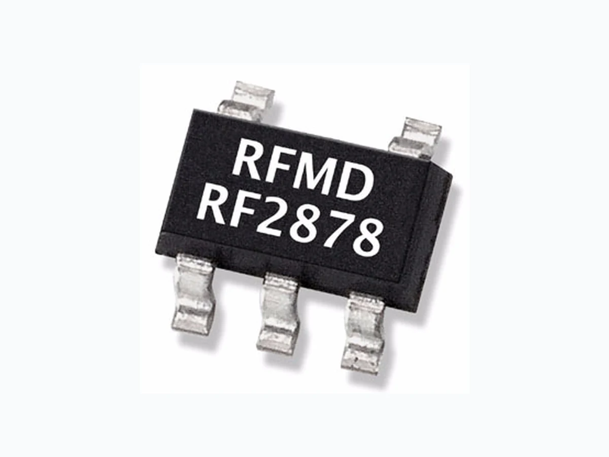
RF2878 QORVO
Document overview
- Manufacturer or author: Provided By www.digicamel.com(FREE DATASHEET DOWNLOAD SITE)
- PDF pages: 14
Technical content
Features
Low Noise and High Intercept Point Adjustable Bias Current Power Down Control Single 2.5V to 5.0V Power Supply 150MHz to 2500MHz Opera- tion
Applications
CDMA/FM Cellular PCS LNA Low Noise Transmit Driver Amplifier General Purpose Amplifica- tion Commercial and Consumer Systems RF2878 Sample bag with 25 pieces RF2878SR 7" Sample reel with 100 pieces RF2878TR7 7" Reel with 2500 pieces RF2878PCK-410 1800MHz to 2170MHz PCBA with 5-piece sample bag DS111104 Package Style: SOT 5-Lead
7628 Thorndike Road, Greensboro, NC 27409-9421 · For sales or technical
support, contact RFMD at (+1) 336-678-5570 or sales-support@rfmd.com . Absolute Maximum Ratings Parameter Rating Unit Supply Voltage, VCC <5V Power Down Voltage, VPD <3V Input RF Level +10 dBm Operating Ambient Temperature -40 to +85 °C Storage Temperature -40 to +150 °C Operating Junction Temperature 150 °C I CC 30 mA Parameter Specification Unit ConditionMin. Typ. Max. Overall RF Frequency Range 150 2500 MHz Low Noise Amplifier 881MHz Performance Schematic per LNA Application; T=25°C, RF=881MHz, V PD=2.8V, R1=1k Gain 20 dB V CC=3.0V, ICC=7 .6mA 20 dB V CC=2.7V, ICC=7 .5mA Noise Figure 1.4 1.6 dB V CC=3.0V, ICC=7 .6mA 1.4 1.6 dB V CC=2.7V, ICC=7 .5mA Input IP3 +6.0 dBm V CC=3.0V, ICC=7 .6mA +5.5 dBm V CC=2.7V, ICC=7 .5mA Low Noise Amplifier 1950MHz Performance Schematic per LNA Application; T=25°C, RF=1950MHz, V PD=2.8V , R1=1k Gain 13 dB V CC=3.0V, ICC=6.4mA 13 dB V CC=2.7V, ICC=6.3mA Noise Figure 1.3 1.5 dB V CC=3.0V, ICC=6.4mA 1.3 1.5 dB V CC=2.7V, ICC=6.3mA Input IP3 +16.5 dBm V CC=3.0V, ICC=6.4mA +1 6.0 dBm V CC=2.7V, ICC=6.3mA Driver Amplifier 836MHz Performance Schematic per Driver Amplifier Application; T=25°C, RF=836MHz, V PD=2.8V Gain 19.5 20.5 21.5 dB V CC=3.5V 19.5 20.5 21.5 dB V CC=3.0V 19.5 20.5 21.5 dB V CC=2.7V Output IP3 25 +32.0 35 dBm V CC=3.5V +29.0 dBm V CC=3.0V +27.8 dBm V CC=2.7V Noise Figure 1.9 2.0 dB V CC=3.5V 1.85 2.0 dB V CC=3.0V 1.8 2.0 dB V CC=2.7V Reverse Isolation 25 dB V CC=3.5V 25 dB V CC=3.0V 25 dB V CC=2.7V Caution! ESD sensitive device. Exceeding any one or a combination of the Absolute Maximum Rating conditions may cause permanent damage to the device. Extended application of Absolute Maximum Rating conditions to the device may reduce device reliability. Specified typical perfor- mance or functional operation of the device under Absolute Maximum Rating condi- tions is not implied. RoHS status based on EUDirective2002/95/EC (at time of this document revision). The information in this publication is believed to be accurate and reliable. However, no responsibility is assumed by RF Micro Devices, Inc. ("RFMD") for its use, nor for any infringement of patents, or other rights of third parties, resulting from its use. No license is granted by implication or otherwise under any patent or patent rights of RFMD. RFMD reserves the right to change component circuitry, recommended appli- cation circuitry and specifications at any time without prior notice.
support, contact RFMD at (+1) 336-678-5570 or sales-support@rfmd.com . Parameter Specification Unit ConditionMin. Typ. Max. Driver Amplifier 836MHz Performance, cont. Input VSWR 1.8:1 2.0:1 Output VSWR 1.25:1 2.0:1 Using External LC network used on evaluation board. P1dB 14.4 dBm V CC=3.5V 12.5 dBm V CC=3.0V 11.5 dBm V CC=2.7V Power Supply T=2 5 ° C Voltage (VCC) 3.5 V Voltage (VPD) 2.8 V Current Consumption - Driver Amplifier (see note 1) Power Down 10 AV CC=3.5V; V PD 0.9 V Driver Amplifier 1880MHz Performance Schematic per Driver Amplifier Application; T=25°C, RF=1880MHz, V PD=2.8V Gain 14.0 dB V CC=3.5V 14.0 dB V CC=3.0V 14.0 dB V CC=2.7V Output IP3 +35.0 dBm V CC=3.5V +31.0 dBm V CC=3.0V +28.8 dBm V CC=2.7V Noise Figure 1.85 2.0 dB V CC=3.5V 1.8 2.0 dB V CC=3.0V 1.75 2.0 dB V CC=2.7V Reverse Isolation 19 dB V CC=3.5V 19 dB V CC=3.0V 19 dB V CC=2.7V Input VSWR 1.6:1 2.0:1 Output VSWR 1.6:1 2.0:1 Using External LC network used on evaluation board. P1dB 14 15.6 dBm V CC=3.5V 13 14.1 dBm V CC=3.0V 12 13.1 dBm V CC=2.7V Power Supply T=2 5 ° C Voltage (VCC) 3.5 V Voltage (VPD) 2.8 V Current Consumption - Driver Amplifier (see note 2) 14 21 29 mA V CC=3.5V; V PD=2.8V Power Down 10 AV CC=3.5V; V PD 0.9 V Note 1: Current consumption shown for ICC only. IPD typical=2.0mA with V PD=2.8V
support, contact RFMD at (+1) 336-678-5570 or sales-support@rfmd.com . Package Drawing Notes: 1.Shaded Lead is Pin 1. 2.Dimensions do not influde mold flash, protrusions or burrs. 3.:ead Dimensions include solder plating. 4.Foot Length measured reference to flat foot surface parallel to datum “A”. 5.Package is die down configuration. Pin Function Description Interface Schematic 1R F I N RF input pin. This pin is DC coupled and matched to 50 at 836 MHz. 2G N D 1 Ground connection. Keep traces physically short and connect immediately to ground plane for best performance. 3V P D For low noise amplifier applications, this pin is used to control the bias current. See plots for bias current settings. An external resistor (R1) can be used to set the bias current for any V PD voltage. For driver amplifier applications, this is the Power Down pin for the IC. VPD=2.8V +/- 0.1V is required for proper operation. VPD< 0.9V turns off the Part. External RF bypass- ing is required. The trace length between the pin and the bypass capacitors should be minimized. The ground side of the bypass capacitors should connect immediately to ground plane. Nominal current required for VPD=2.8V is 2.0mA typical and 3.0mA Max (@ VPD=2.9V). 4R F O U T Amplifier Output pin. This pin is an open-collector output. It must be biased to either VCC or pin 4 through a choke or matching inductor. This pin is typically matched to 50 with a shunt bias/matching inductor and series blocking/matching capacitor. Refer to appli- cation schematics. 5G N D 2 Ground connection. Keep traces physically short and connect immediately to ground plane for best performance. RF IN RF OUT To Bias Circuit PD 1.60±.10 2.90±.10 2.80±.20 .520 .360 TYP .950 .45±.10 1.44 1.04 .15 .05 3°MAX 0°MIN -A- .127 TYP 10° TYP 1.14±.15
support, contact RFMD at (+1) 336-678-5570 or sales-support@rfmd.com . Application Schematic: 350MHz LNA Application Schematic: 350MHz Linear Driver 22 nF RF IN 220 pF10 nF 1 k VPD 39 nH 4 pF RF OUT 220 pF 10 nF VCC VCC=3.5V, VPC=2.8V ICC=7mA Gain=25.5dB NF=1.75dB IIP3=-4.5dBm S11=-2.8dB S22=-10.4dB 22 nF RF IN 220 pF 10 nF 0 VPD 39 nH 4.3 pF RF OUT 220 pF 10 nF VCC VCC=3.5V, VPC=2.7V ICC=20mA Gain=26dB OIP3=27.5dBm OP1dB=13.8dBm S11=S22=-14dB 50 strip 50 strip 50 strip 510 56 nH
support, contact RFMD at (+1) 336-678-5570 or sales-support@rfmd.com . Application Schematic: 1200MHz to 1600MHz Driver (set resistance at VPD=1000 for LNA) Application Schematic: 1800MHz to 2170MHz Linear Driver (set resistance at VPD=1000 for LNA) 22 nF RF IN 100 pF10 nF 0 VPD 6.8 nH 1.5 pF RF OUT 100 pF 10 nF VCC VCC=3.5V, VPC=2.7V ICC=21mA Gain=17dB to 14.2dB from 1200MHz to 1600MHz S11=-8.7dB to -23dB from 1200MHz to 1600MHz S22=-14.5dB to -8.1dB from 1200MHz to 1600MHz 22 nF RF IN 100 pF10 nF 0 VPD 2.7 nH 1 pF RF OUT 100 pF 10 nF VCC VCC=4V, VPC=2.7V ICC=21mA Gain=13.8dB to 12.3dB from 1800MHz to 2170MHz S11=-11dB to -20dB from 1800MHz to 2170MHz S22=-11.5dB to -12.5dB from 1800MHz to 2170MHz OIP3=36dBm to 34.5dBm from 1800MHz to 2170MHz OP1dB=16dBm to 17dBm from 1800MHz to 2170MHz 47 47 dropping R for use with VCC=5V. 5-0.021*47=4V at RF2878 collector
support, contact RFMD at (+1) 336-678-5570 or sales-support@rfmd.com . Application Schematic: Low Noise Amplifier ~1950MHz Operation Application Schematic: Driver Amplifier ~1880MHz Operation 22 nF RF IN 100 pF10 nF 1k VPD 3.3 nH 1 pF RF OUT 100 pF 10 nF VCC 22 nF RF IN 100 pF10 nF 0 VPD 3.3 nH 1 pF RF OUT 100 pF 10 nF VCC
support, contact RFMD at (+1) 336-678-5570 or sales-support@rfmd.com . Evaluation Board Schematic: Low Noise Amplifier ~881MHz Operation Evaluation Board Schematic: Driver Amplifier ~836MHz Operation 22 nF50 stripJ1 RF IN 220 pF 10 nF 1k VPD 50 strip 2 pF 50 strip J2 RF OUT 12 nH 220 pF 10 nF VCC2361410 Rev- P1-1 VPD GND 4.7 F VCC 22 nF50 stripJ1 RF IN 220 pF 10 nF 0 VPD 50 strip 2 pF 50 strip J2 RF OUT 12 nH 220 pF 10 nF VCC2361400 Rev- P1-1 VPD GND VCC 4.7 F
support, contact RFMD at (+1) 336-678-5570 or sales-support@rfmd.com . Evaluation Board Layout - 900MHz Driver Board Size 0.948” x 1.063” Board Thickness 0.031”; Board Material FR-4 Evaluation Board Layout - 900MHz LNA
support, contact RFMD at (+1) 336-678-5570 or sales-support@rfmd.com . Theory of Operation This section will focus on a variety of applications outside th e nominal, for the purpose of demonstrating RF2878 versatility. Application schematics pertaining to topics discussed can be found within the data sheet for reference. First, an application for linear driver, covering 1800MHz to 2170MHz. Operating condition: VCC=4V VPD=2.7V ICC=2 1mA Note 0 value for bias resistor at VPD in the application schematic, set for increased current/IP3. Typical specs are listed along with schematic. VCC=4V contributes to enhanced compression point (16dBm to 17dBm). Junction temperature seen for ambi- ent condition=85°C will be a consideration in setting V CC/VPD. The above biasing condition yields TJ=132°C. Thus, the condi- tions chosen allow for highly reliable operation while providing impressive linear performance. Using a 5V supply rail is often convenient from a design standpoint. In the 1800MHz to 2170MHz driver application already discussed, VCC=4V is recommended in order to maintain highest reliability. An option for using V CC=5V is shown in the appli- cation schematic. Use of a simple dropping resistor at V CC provides 4.0V at output collector, resulting in the suggested device operating condition. Power dissipation in the resistor=0.021 Watt, easily handled by standard resistors available to the system designer. Moving to another application, consider the schematic for 350MHz LNA. Noise figure in this case=1.75dB. In contrast to above linear driver, bias resistor is set at 1000 to limit current. In the specifications next to schematic, see that input return loss is somewhat degraded at 2.8dB. The absence of input matching is intentional, as the integrated circuit design was geared for optimum noise figure with input looking back into 50 . Note that in the nominal cases, 881MHz and 1950MHz, input return losses are favorable in the absence of input match. In converting 350MHz LNA to driver , noise figure will no longer be a key specification. As such, RF2878 device s-parameter data can be used to match input for favorable return loss. The resulting driver application schematic is found below that for the LNA. When matching in bands other than those covered here, RF2878 S-parameter data can be obtained through applica- tions/sales contact at RFMD. As a final example, refer to driver application schematic covering 1200MHz to 1600MHz. This match provides favorable return losses over the entire band. In summary, the examples above are intended to aid the system designer in determining suitable matches and device operat- ing points for both LNA and driver applications. Key points to consider: 1. In setting bias condition to accommodate both LNA and driver , the first consideration is choice of bias resistance at VPC. Linearity versus power dissipation trade-offs are taken into account in the driver application. 2. Noise figure versus input return loss trade-off must be consid ered in the specific case of low frequency LNA application. Driver application here allows for flexibility in optimizing input match for return loss. 3. Higher frequency LNA sees favorable return loss in the abse nce of input match. Thus, optimization at frequency >800MHz involves matching adjust to output L-C only. 4. Small signal S-parameter simulation proves an excellent method for obtaining starting point matches in the design process.
support, contact RFMD at (+1) 336-678-5570 or sales-support@rfmd.com . Driver Amp 836 MHz ICC versus VPD 19.0 19.5 20.0 20.5 21.0 21.5 22.0 22.5 23.0 23.5 24.0 24.5 25.0 25.5 26.0 0.39.28.27.2 VPD ICC (mA) 2.7V Icc (mA) 3.0V Icc (mA) 3.3V Icc (mA) 3.6V Icc (mA) Driver Amp 836 MHz Gain versus VPD 20.72 20.74 20.76 20.78 20.80 20.82 20.84 20.86 20.88 20.90 20.92 2.70 2.80 2.90 3.00 VPD Gain (dB) 2.7V Gain (dB) 3.0V Gain (dB) 3.3V Gain (dB) 3.6V Gain (dB) Driver Amp 836 MHz OIP3 versus VPD 27.0 28.0 29.0 30.0 31.0 32.0 33.0 0.39.28.27.2 VPD OIP3 (dBm) 2.7V OIP3 (dBm) 3.0V OIP3 (dBm) 3.3V OIP3 (dBm) 3.6V OIP3 (dBm) Driver Amp 836 MHz POUT 1dB versus VPD 11.0 11.5 12.0 12.5 13.0 13.5 14.0 14.5 15.0 0.39.28.27.2 VPD POUT 1dB (dBm) 2.7V P 1dB (dBm) 3.0V P 1dB (dBm) 3.3V P 1dB (dBm) 3.6V P 1dB (dBm) Driver Amp 836 MHz Noise Figure versus VPD 1.70 1.75 1.80 1.85 1.90 1.95 2.00 2.05 2.70 2.80 2.90 3.00 VPD NF (dB) 2.7V NF (dB) 3.0V NF (dB) 3.3V NF (dB) 3.6V NF (dB)
support, contact RFMD at (+1) 336-678-5570 or sales-support@rfmd.com . Low Noise Amplifier 881 MHz Gain versus ICC 19.55 19.60 19.65 19.70 19.75 19.80 19.85 19.90 19.95 ICC Gain (dB) 2.7V Gain (dB) 3.0V Gain (dB) 3.3V Gain (dB) 3.6V Gain (dB) Low Noise Amplifier 881 MHz OIP3 versus ICC 24.0 24.5 25.0 25.5 26.0 26.5 27.0 27.5 28.0 28.5 29.0 ICC (mA) OIP3 (dBm) 2.7V OIP3 (dBm) 3.0V OIP3 (dBm) 3.3V OIP3 (dBm) 3.6V OIP3 (dBm) Low Noise Amplifier 881 MHz IIP3 versus ICC 4.0 4.5 5.0 5.5 6.0 6.5 7.0 7.5 8.0 8.5 9.0 ICC (mA) IIP3 (dBm) 2.7V IIP3 (dBm) 3.0V IIP3 (dBm) 3.3V IIP3 (dBm) 3.6V IIP3 (dBm) Low Noise Amplifier 881 MHz POUT 1dB versus ICC 9.5 10.0 10.5 11.0 11.5 12.0 12.5 13.0 13.5 ICC (mA) POUT 1dB (dBm) 2.7V Pout 1dB (dBm) 3.0V Pout 1dB (dBm) 3.3V Pout 1dB (dBm) 3.6V Pout 1dB (dBm) Low Noise Amplifier 881 MHz Noise Figure versus ICC 1.33 1.34 1.35 1.36 1.37 1.38 1.39 1.40 1.41 1.42 ICC NF (dB) 2.7V NF (dB) 3.0V NF (dB) 3.3V NF (dB) 3.6V NF (dB)
support, contact RFMD at (+1) 336-678-5570 or sales-support@rfmd.com . to 8inch gold over 180inch nickel. cesses. The PCB land pattern has been developed to accommodate lead and package tolerances. Figure 1. PCB Metal Land Pattern (Top View)
support, contact RFMD at (+1) 336-678-5570 or sales-support@rfmd.com . provided in the master data or requested from the PCB fabrication supplier. Figure 2. PCB Solder Mask (Top View) suppliers, and applies to the Bill of Materials (BOM) revision noted above.