
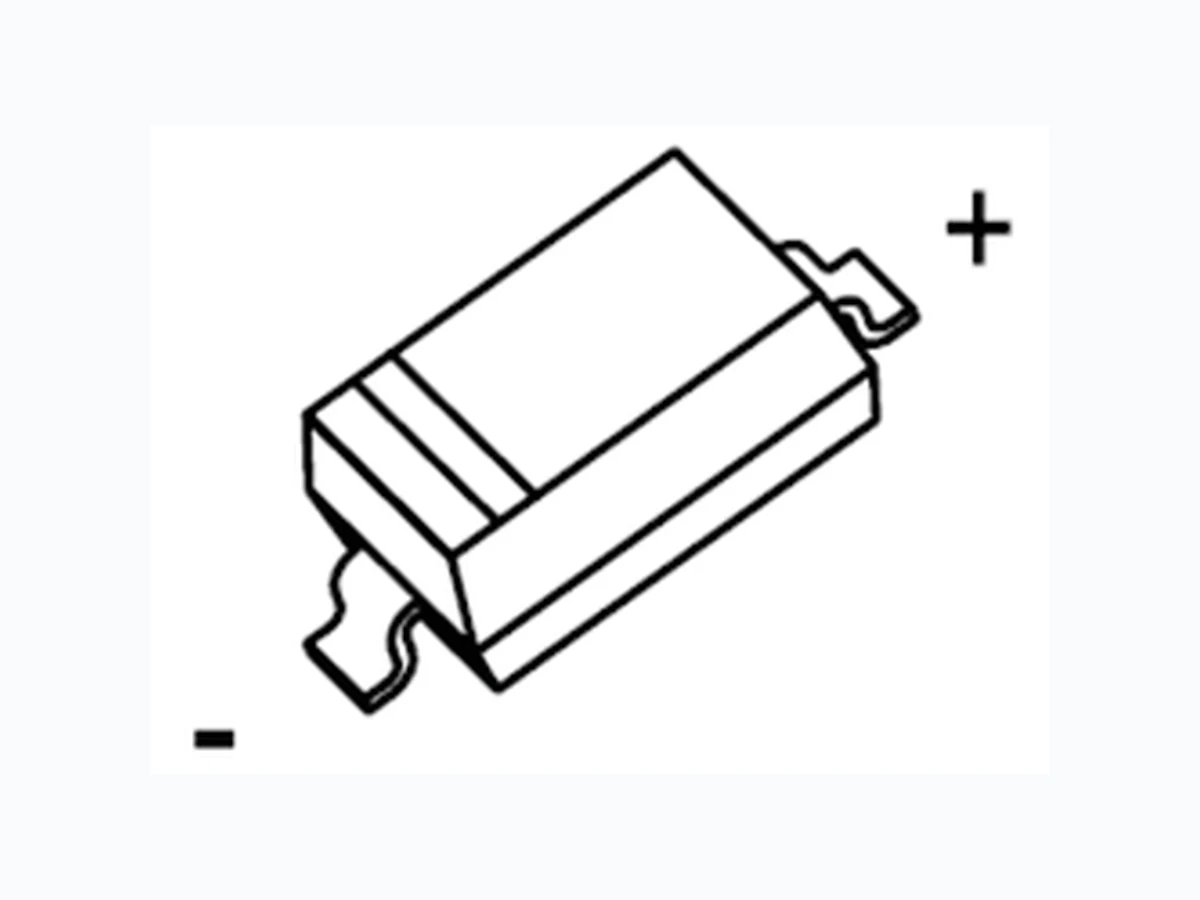
RB160M-60 JIANGSU
Document overview
- Manufacturer or author: Provided By www.digicamel.com(FREE DATASHEET DOWNLOAD SITE)
- PDF pages: 4
Technical content
JIANGSU CHANGJIANG ELECTRONICS TECHNOLOGY CO., LTD SOD-123 Plastic-Encapsulate Diodes RB160M-60 Schottky Barrier Diode
FEATURES
/g122 Small Power Mold Type /g122 Low I R /g122 High Reliability MARKING: 76 Maximum Ratings @Ta =25/g1071 Parameter Symbol Limit Unit DC reverse voltage V R 60 V Mean rectifying current I O 1 A Peak forward surge current @t=8.3ms I FSM 15 A Electrical characteristics @T a =25/g1071 Parameter Symbol Min. Typ. Max. Unit Conditions Forward voltage V F
0.58 V I
F =1A Reverse current I R 30 A V R =60V SOD-123 Junction temperature T j 150 /g1071 Storage temperature T stg -55~+150 /g1071 /g51/g82/g90/g72/g85/g3/g71/g76/g86/g86/g76/g83/g68/g87/g76/g82/g81P D/g3/g3/g3/g3/g3/g3/g3/g3/g3/g3/g3/g3/g3/g3/g3/g3/g3/g3/g3/g3/g3/g3/g3/g3/g3/g3/g3/g3/g3/g3/g3/g3/g3/g3/g3/g3/g3/g3/g3/g3/g3/g3/g3/g3/g3/g3/g3/g3/g3/g3/g3/g3/g3/g3/g3/g3/g3/g3/g3/g3/g3/g3/g3/g3/g3/g3/g3/g3/g3 /g3/g3/g3/g3/g22/g24/g19 mW /g55/g75/g72/g85/g80/g68/g79/g3/g53/g72/g86/g76/g86/g87/g68/g81/g70/g72/g3/g45/g88/g81/g70/g87/g76/g82/g81/g3/g87/g82/g3/g36/g80/g69/g76/g72/g81/g87/g3 /g3/g3 R θ JA /g3/g3 /g3/g3/g3/g3/g3/g3/g3/g3/g3/g3/g3/g3/g3/g3/g3/g3/g3/g3/g3/g3/g3/g3/g3/g3/g3/g3/g3/g3/g3/g3/g3/g3/g3/g3/g3/g3/g3/g3/g3/g3/g3/g3/g3/g3/g3/g3/g3/g3/g3/g3/g3/g3/g3/g3/g3/g3/g3/g3/g3/g3/g3/g3/g3/g3 /g3 /g3 /g21/g27/g25 /g3/g3/g3/g1071/W /g90/g90/g90/g17/g70/g77/g16/g72/g79/g72/g70/g17/g70/g82/g80/g3/g3/g3/g3/g3/g3/g3/g3/g3/g3/g3/g3/g3/g3/g3/g3/g3/g3/g3/g3/g3/g3/g3/g3/g3/g3/g3/g3/g3/g3/g3/g3/g3/g3/g3/g3/g3/g3/g3/g3/g3/g3/g3/g3/g3/g3/g3/g3/g3/g3/g3/g3/g3/g3/g3/g3/g3/g3/g3/g3/g3/g3/g3/g3/g3/g3/g3/g3/g20/g3/g3/g3/g3/g3/g3/g3/g3/g3/g3/g3/g3/g3/g3/g3/g3/g3/g3/g3/g3/g3/g3/g3/g3/g3/g3/g3/g3/g3/g3/g3/g3/g3/g3/g3/g3/g3/g3/g3/g3/g3/g3/g3 The marking bar indicates the cathode Solid dot = Green molding compound device,if none, the normal device. D,Mar,2015
0.1 100 1000 0 5 10 15 20 25 30 100 150 200 250 Power Derating Curve POWER DISSIPATION P D (mW) AMBIENT TEMPERATURE T a ( ) ć T a =25 ć T a =100 ć REVERSE CURRENT I R (uA) REVERSE VOLTAGE V R (V) Reverse Characteristics Pulsed Pulsed Forward Characteristics FORWARD VOLTAGE V F (mV) FORWARD CURRENT I F (mA) T a =25 ć T a =100 ć Capacitance Characteristics T a =25 ć f=1MHz CAPACITANCE BETWEEN TERMINALS C T (pF) REVERSE VOLTAGE V R (V) /g55/g92/g83/g76/g70/g68/g79/g3/g38/g75/g68/g85/g68/g70/g87/g72/g85/g76/g86/g87/g76/g70/g86 /g3/g3/g3/g3/g3/g3/g3/g3/g3/g3/g3/g3/g3/g3/g3/g3/g3/g3/g3/g3/g3/g3/g3/g3/g3/g3/g3/g3/g3/g3/g3/g3/g3/g3/g3/g3/g3/g3/g3/g3/g3/g3/g3/g3/g3/g3/g3/g3/g3/g3/g3/g3/g3/g3/g3/g3/g3/g3/g3/g3/g3/g3/g3/g3/g3/g3/g3/g3/g3/g3/g3/g3/g3/g3/g3/g3/g3/g3/g3/g3/g3/g3/g3/g3/g3/g3/g3/g3/g3/g3/g3/g3/g3/g3/g3/g3/g3/g3/g3/g3/g3/g3/g3/g3/g3/g3/g3/g3/g3/g3/g3/g3/g3/g3/g3/g3/g3/g3/g3/g3/g3/g3/g3/g3/g3/g3/g3/g3/g3/g3/g3 /g90/g90/g90/g17/g70/g77/g16/g72/g79/g72/g70/g17/g70/g82/g80/g21 D,Mar,2015
www.cj-elec.com 3 SOD-123 Suggested Pad Layout Min Max Min Max A 1.050 1.250 0.041 0.049 A1 0.000 0.100 0.000 0.004 A2 1.050 1.150 0.041 0.045 b 0.450 0.650 0.018 0.026 c 0.080 0.150 0.003 0.006 D 1.500 1.700 0.059 0.067 E 2.600 2.800 0.102 0.110 E1 3.550 3.850 0.140 0.152 L L1 0.250 0.450 0.010 0.018 θ 0° 8° 0° 8° 0.500 REF 0.020 REF Symbol Dimensions In Millimeters Dimensions In Inches D,Mar,2015
www.cj-elec.com 4 D,Mar,2015 SOD-123 Tape and Reel