
3 A step-down switching regulator for aerospace applications
Document overview
- Manufacturer or author: STMICROELECTRONICS
- PDF pages: 37
Technical content
Datasheet sections
- 1 Pin settings
- 1.1 Pin connection
- 1.2 Pin description
- 2 Maximum ratings
- 3 Thermal data
- 4 Electrical characteristics
- 5 Functional description
- 5.1 Oscillator and synchronization
- 5.2 Soft-start
- 5.3 Error amplifier and compensation
- 5.4 Overcurrent protection
- 5.5 Enable function
- 5.6 Hysteretic thermal shutdown
- 6 Application information
- 6.1 Input capacitor selection
- 6.2 Inductor selection
- 6.3 Output capacitor selection
- 6.4 Compensation network
- 6.4.1 Type III compensation network
- 6.4.2 Type II compensation networ k
- 6.5 Thermal considerations
- 6.6 Layout considerations
- 7 Application ideas
- 7.1 Positive buck-boost
- 7.2 Inverting buck-boost
Features
General features – 3 A DC output current – 4.5 V to 38 V input voltage – Large ambient temperature range: -40 °C to 125 °C – Output voltage adjustable from 0.6 V – 250 kHz switching frequency, programmable up to 1 MHz – Internal soft-start and enable – Low dropout operation: 100% duty cycle – Voltage feed-forward – Zero load current operation – Overcurrent and thermal protection – HSOP8 package Aerospace and defense features – Suitable for use in aerospace and defense
applications
– Dedicated traceabilit y and part marking – Production parts approval documents available – Adapted extended life time and obsolescence management – Extended product change notification process – Designed and manufactured to meet sub- ppm quality goals – Advanced mold and frame designs for superior resilience in harsh environments (acceleration, EMI, thermal, humidity) – Extended screening ca pability on request Dedicated to aerospace applications Aerospace LED driving
Description
The R7986A is a step-down switching regulator with a 3.7 A (min.) current limited embedded power MOSFET, so it is able to deliver up to 3 A current to the load depending on the application conditions. The input voltage can range from 4.5 V to 38 V, while the output voltage can be set starting from
0.6 V to V
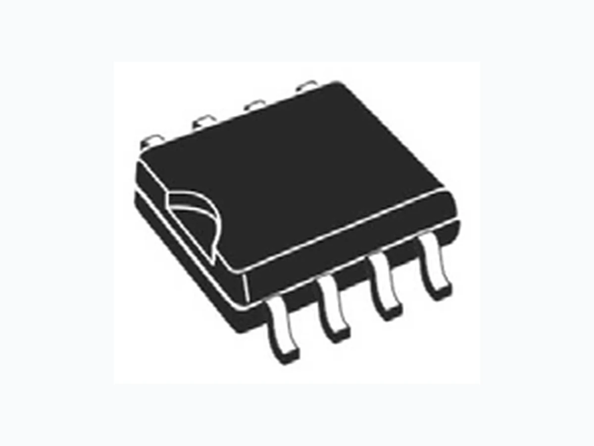
IN. Requiring a minimum set of external components, the device includes an internal 250 kHz switching frequency oscillator that can be externally adjusted up to 1 MHz. The large ambient temperature range makes it ideal for aerospace and defense applications. The HSOP8 package with exposed pad allows the reduction of R th(JA) down to 40 °C/W. HSOP8 exposed pad
1 Pin settings
1.1 Pin connection
Figure 1. Pin connection (top view)
1.2 Pin description
Table 1. Pin description
2 SYNCH
powers turn-ons have a phase shift of half a period. 1.2 V the device is ON and with EN lower than 0.3 V the device is OFF. 4 COMP Error amplifier output to be used for loop frequency compensation. external resistor divider is required from VOUT to the FB pin. works at its free-running frequency of 250 KHz. CC Unregulated DC input voltage.
2 Maximum ratings
3 Thermal data
Table 2. Absolute maximum ratings Table 3. Thermal data
- Package mounted on demonstration board.
4 Electrical characteristics
TJ = - 40 °C to 125 °C, VCC = 12 V, unless otherwise specified. Table 4. Electrical characteristics
Table 4. Electrical characteristics (continued)
5 Functional description
off time of the power switch. synchronization signal. Its switching frequency can be adjusted by an external resistor. A thermal shutdown block, to prevent thermal runaway. Figure 2. Block diagram
5.1 Oscillator and synchronization
shown in Figure 5 by an external resistor connected to ground. according to the input voltage change (see Figure 4.a). flowing through the input capacitor (see the L5988D datasheet). Figure 3. Oscillator circuit block diagram sawtooth negligible, due to the external synchronization.
5.2 Soft-start
avoids inrush current surge and makes the output voltage increase monothonically. 64 steps of 9.5 mV each, from 0 V to 0.6 V. The time base of one step is of 32 clock cycles. Figure 6. Soft-start scheme
5.3 Error amplifier and compensation
mode operational amplifier so with high DC gain and low output impedance. compensation network selection).
5.4 Overcurrent protection
time” or “blanking time”. The masking time is about 200 ns. skips two pulses. This mechanism is repeated and the device can skip up to seven pulses. the number of skipped cycles is decreased by one unit (see Figure 7). order to keep constant the output current around the current limit. Table 5. Uncompensated error amplifier characteristics
R7986A Functional description This kind of overcurrent protection is effective if the output current is limited. To prevent the current from diverging, the current ripple in the inductor during the on-time must not be higher than the current ripple during the off-time. That is: Equation 3 If the output voltage is shorted, VOUT 0, IOUT = ILIM, D/FSW = TON_MIN, (1-D)/FSW 1/FSW. So, from the above equation, the maximum switching frequency that guarantees to limit the current results: Equation 4 With RDS(on) = 300 m, DRC = 0.08 , the worst condition is with VIN = 38 V, ILIM = 3.7 A; the maximum frequency to keep the output current limited during the short-circuit results 88 kHz. Based on the pulse-by-pulse mechanism, that reduces the switching frequency down to one eighth, the maximum F SW, adjusted by the FSW pin, which assures that a full effective output current limitation is 88 kHz * 8 = 706 kHz. If, with VIN= 38 V, the switching frequency is set higher than 706 kHz, during short-circuit condition the system finds a different equilibrium with higher current. For example, with FSW = 800 kHz and the output shorted to ground, the output current is limited around: Equation 5 where FSW* is 800 kHz divided by eight. VIN V– OUT RDSON IOUT DCR I OUT–– VOUT VF RDSON IOUT DCR I OUT++ + FSW * VF DCR I+ LIM TON_MIN IOUT
Figure 7. Overcurrent protection
5.5 Enable function
than 0.3 V the device is disabled and the power consumption is reduced to less than 30A. device is disabled. The pin is also VCC compatible.
5.6 Hysteretic thermal shutdown
area, so ensuring an accurate and fast temperature detection.
6 Application information
Figure 8. Application circuit
6.1 Input capacitor selection
affecting the overall system efficiency. input current and an ESR value compliant with the expected efficiency. o is the maximum DC output current, D is the duty cycle, and is the efficiency. Considering , this function has a maximum at D = 0.5 and is equal to Io/2.
where ESR is the equivalent series resistance of the capacitor. neglecting the small ESR of ceramic capacitors. Table 6. Input MLCC capacitors
6.2 Inductor selection
minimum inductance value, in order to have the expected current ripple, must be selected. The rule to fix the current ripple value is to have a ripple at 20% - 40% of the output current. where FSW is the switching frequency, 1/(TON + TOFF). inductance value to have IL= 30% of IO is about 18 H. output current that can be delivered, without triggering the overcurrent protection. In Table 7 some inductor part numbers are listed. Table 7. Inductors
6.3 Output capacitor selection
must be chosen in order to sustain the load transient. In Table 8 some capacitor series are listed. Table 8. Output capacitors
6.4 Compensation network
EA is considered as ideal, that is, its bandwidth is much larger than the system one. changes and how to keep it constant in spite of the external synchronization). Figure 9. The error amplifier, the PWM modulation and the LC output filter
Application information R7986A The transfer function on the LC filter is given by: Equation 19 where: Equation 20 Equation 21 As seen in Section 5.3 on page 12, two different kinds of network can compensate the loop. In the two following paragraphs, the guidelines to select the Type II and Type III compensation network are illustrated.
6.4.1 Type III compensation network
The methodology to stabilize the loop consists of placing two zeros to compensate the effect of the LC double pole, therefore increasing phase margin; then to place one pole in the origin to minimize the DC error on regulated output voltage; finally, to place other poles far from the zero dB frequency. If the equivalent series resistance (ESR) of the output capacitor introduces a zero with a frequency higher than the desired bandwidth (that is: 2ESR COUT < 1 / BW), the Type III compensation network is needed. Multi-layer ceramic capacitors (MLCC) have very low ESR (< 1 m), with very high frequency zero, so a Type III network is adopted to compensate the loop. In Figure 10, the Type III compensation network is shown. This network introduces two zeros (fZ1, fZ2) and three poles (fP0, fP1, fP2). They are expressed as: Equation 22 Equation 23 GLC s 1 s 1 s 2 fLC 2 LC OUT 1 ESR ROUT Q ROUT LC OUT ROUT ESR+ VOUT IOUT fZ1 fP0 0= fP1 2 R4 C4 C5
Application information R7986A Equation 25 4. Calculate C 5 by placing the second pole at four times the system bandwidth (BW): Equation 26 5. Set also the first pole at four times th e system bandwidth and also the second zero at the output filter double pole: Equation 27 The suggested maximum system bandwidth is equal to the switching frequency divided by 3.5 (FSW/3.5), anyway lower than 100 kHz if the FSW is set higher than 500 kHz. For example, with VOUT = 5 V, VIN = 24 V, IO = 3 A, L = 18 H, COUT = 22 F, and ESR<1 m, the Type III compensation network is: Equation 28 In Figure 12, the module and phase of the open loop gain is shown. The bandwidth is about 32 kHz and the phase margin is 51°. 4B W fLC
Figure 12. Open loop gain Bode diagram with ceramic output capacitor
6.4.2 Type II co mpensation network
the stabilization of the loop.
The guidelines for positioning the poles and the zeroes and for calculating the component values can be summarized as follows: 1. Choose a value for R 1, usually between 1 k and 5 k, in order to have values of C4 and C5 not comparable with parasitic capacitance of the board. 2. Choose a gain (R 4/R1) in order to have the required bandwidth (BW), that means: Equation 30 where fESR is the ESR zero: Equation 31 and Vs is the sawtooth amplitude. The voltage feed-forward keeps the ratio Vs/Vin constant. 3. Calculate C 4 by placing the zero one decade below the output filter double pole: Equation 32 4. Then calculate C 3 in order to place the second pole at four times the system bandwidth (BW): Equation 33 For example with VOUT = 5 V, VIN = 24 V, IO = 3 A, L = 18 H, COUT = 330 F, and ESR = 35 m the Type II compensation network is: In Figure 15, the module and phase of the open loop gain is shown. The bandwidth is about 21 kHz and the phase margin is 45°. fESR fLC 2 BW fESR VS VIN fESR
Figure 15. Open loop gain Bode diagram with electrolytic/tantalum output capacitor
6.5 Thermal considerations
The thermal design is important to prevent the thermal shutdown of the device if junction temperature goes above 150 °C. The three different sources of losses within the device are: a) conduction losses due to the not negligible R DS(on) of the power switch; these are equal to: Equation 34 where D is the duty cycle of the application and the maximum RDS(on) overtemperature is 220 m. Note that the duty cycle is theoretically given by the ratio between VOUT and VIN, but actually it is quite higher to compensate the losses of the regulator. So the conduction losses increase compared with the ideal case. b) switching losses due to power MOSF ET turn ON and OFF; these can be calculated as: Equation 35 where T RISE and TFALL are the overlap times of the voltage across the power switch (VDS) and the current flowing into it during turn ON and turn OFF phases, as shown in Figure 16. TSW is the equivalent switching time. For this device the typical value for the equivalent switching time is 40 ns. c) Quiescent current lo sses, calculated as: Equation 36 where IQ is the quiescent current (IQ= 2.4 mA). The junction temperature TJ can be calculated as: Equation 37 where TA is the ambient temperature and PTOT is the sum of the power losses just seen. Rth(JA) is the equivalent thermal resistance junction to ambient of the device; it can be calculated as the parallel of many paths of heat conduction from the junction to the ambient. For this device the path through the exposed pad is the one conducting the largest amount of heat. The Rth(JA) measured on the demonstration board described in the following paragraph is about 40 °C/W for the HSOP8 package. PSW VIN IOUT TRISE TFALL+ PQ VIN IQ= TJ TA Rth JA PTOT+=
Figure 16. Switching losses
6.6 Layout considerations
be placed very close to the device. close as possible to the input voltage pin of the device. of the converter allowing high power conversion.
In Figure 17, a layout example is shown. Figure 17. Layout example
7 Application ideas
7.1 Positive buck-boost
Figure 18. Positive buck-boost regulator higher than 16 V, the gate must be protected through a Zener diode and resistor). output current for the buck-boost topology can be calculated from Equation 40.
where ISW is the average current in the embedded power MOSFET in the ON time. Equation 41, must be lower than the minimum current limit (3.7 A). input voltage from 4.5 V to 38 V. MOSFET are taken into account. Figure 19. Maximum output current according to max. DC switch current (3.0 A):
7.2 Inverting buck-boost
to the standard buck topology. where the duty cycle is given by Equation 44. Figure 20. Inverting buck-boost regulator
power MOSFET are taken into account. Figure 21. Maximum output current according to switch max. peak current (3.0 A):
8 Package information
specifications, grade definitions and product status are available at: www.st.com. Figure 22. HSOP8 package outline
Table 9. HSOP8 package mechanical data
9 Ordering information
Table 10. Ordering information Table 11. Document revision history 06-Oct-2014 1 In itial release.