

 Download PDF
R7400U_04 HAMAMATSU
Document overview
- PDF pages: 8
Technical content
Page 1

Compact size (16 mm diameter, 12 mm seated length),
Fast Time response (rise time 0.78 ns)
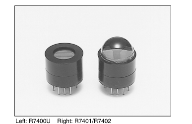
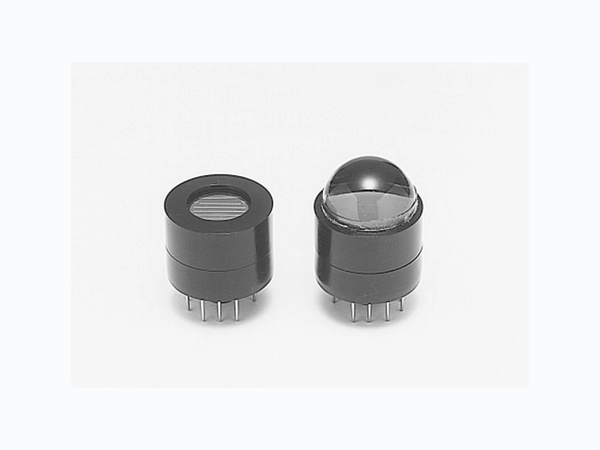
The R7400U series is a subminiature photomultiplier tube with a 16 mm diameter and 12 mm seated length. A precision engi- neered 8-stage electron multiplier (composed of metal channel
dynodes) is incorporated in the TO-8 package to produce a noise free gain of 700,000 times (R7400U). The R7400U series also features excellent response time with a rise time of 0.78 ns. Vari-
ous types of the R7400U series are available with different spec- tral response and gain ranges, including those selected specifi- cally for photon counting applications. Hamamatsu also provides
a lens input option to the series (R7401 and R7402), effectively doubling the active area.
FEATURES
World's smallest photomultiplier tubes assembled. (1/7th of the Hamamatsu R647) The necessary components are built into a TO-8 package while retaining full photomultiplier tube performance to cre-
ate a new generation of photosensors.
Specially selected on account of low noise and high gain. For use in photon counting applications.
The lens window type doubles the effective input area to 12 mm in diameter.
SERIES
| Solar Blind | UV to Visible Range | Visible Range | Visible to Near IR Range | UV to Near IR Range | ||||
| Standard | R7400U-09 | R7400U-03 | R7400U-06 | R7400U | R7400U-01 | R7400U-02 | R7400U-20 | R7400U-04 |
| For Photon Counting | — | — | — | R7400P, R7401P | — | — | — | — |
| With Lens | — | — | — | R7401 | R7402 | R7402-02 | R7402-20 | — |
SPECIFICATIONS
GENERAL
| Parameter | Description/Value | Unit | ||
|---|---|---|---|---|
| Minimum Effective Area | 8 | mm | ||
| Dynode | Structure | Metal Channel | — | |
| Number of Stages | 8 | — | ||
| Weight | Without Lens | Approx. 5.3 | g | |
| With Lens | Approx. 6.3 | g | ||
| Operating Ambient Temperature and Storage Temperature | Without Lens | -80 to +50 | °C | |
| With Lens | -30 to +50 | °C | ||
VOLTAGE DISTRIBUTION RATIO
| Electrodes | K | Dy1 | Dy2 | Dy3 | Dy4 | Dy5 | Dy6 | Dy7 | Dy8 | P | ||||||||||
| Ratio | 1 | 1 | 1 | 1 | 1 | 1 | 1 | 1 | 0.5 | |||||||||||
Supply Voltage: 800 V K: Cathode Dy: Dynode P: Anode
Subject to local technical requirements and regulations, availability of products included in this promotional material may vary. Please consult with our sales office. Information furnished by HAMAMATSU is believed to be reliable. However, no responsibility is assumed for possible inaccuracies or omissions. Specifications are subject to change without notice. No patent rights are granted to any of the circuits described herein. ©2004 Hamamatsu Photonics K.K.
Page 2
CHARACTERISTICS (at 25 °C)
| Type No. | Remarks | Spectral Response | Photo- cathode Material | Window Material | Out-(a) line No. | Maximum Ratings | Cathode Characteristics | ||||||
|---|---|---|---|---|---|---|---|---|---|---|---|---|---|
| Range (nm) | Peak Wave- Iength (nm) | Anode to Cathode Voltage (V) | Average Anode Current(b) (mA) | Luminous | Blue Sensitivity Index (CS 5-58) Typ. | Red/White Ratio (R-68) Typ. | Radiant Typ. (mA/W) | ||||||
| Min. (µA/lm) | Typ. (µA/lm) | ||||||||||||
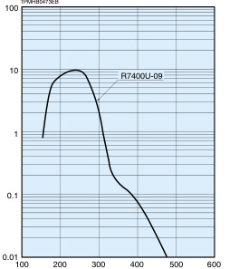
| R7400U-09 | Solar Blind | 160 to 320 | 240 | Cs-Te | Synthetic silica | w | 1000 | 0.01 | — | — | — | — | 10(c) |
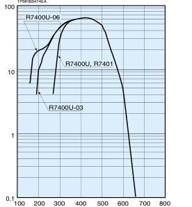
| R7400U | Visible | 300 to 650 | 420 | Bialkali | Borosilicate glass | q | 1000 | 0.1 | 40 | 70 | 8 | — | 62 |
| R7400U-03 | UV to Visible | 185 to 650 | 420 | Bialkali | UV glass | q | 1000 | 0.1 | 40 | 70 | 8 | — | 62 |
| R7400U-06 | UV to Visible | 160 to 650 | 420 | Bialkali | Synthetic silica | w | 1000 | 0.1 | 40 | 70 | 8 | — | 62 |
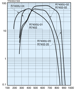
| R7400U-01 | Visible to Near IR | 300 to 850 | 400 | Multialkali | Borosilicate glass | q | 1000 | 0.1 | 80 | 150 | — | 0.20 | 60 |
| R7400U-02 | Visible to Near IR | 300 to 880 | 500 | Multialkali | Borosilicate glass | q | 1000 | 0.1 | 200 | 250 | — | 0.25 | 58 |
| R7400U-20 | Visible to Near IR | 300 to 920 | 630 | Multialkali | Borosilicate glass | q | 1000 | 0.1 | 350 | 500 | — | 0.45 | 78 |
| R7400U-04 | UV to Near IR | 185 to 850 | 400 | Multialkali | UV glass | q | 1000 | 0.1 | 80 | 150 | — | 0.20 | 60 |
| R7401 | With Lens | 300 to 650 | 420 | Bialkal | Borosilicate glass | e | 1000 | 0.1 | 40 | 70 | 8 | — | 62 |
| R7402 | With Lens | 300 to 850 | 400 | Multialkali | Borosilicate glass | e | 1000 | 0.1 | 80 | 150 | — | 0.20 | 60 |
| R7402-02 | With Lens | 300 to 880 | 500 | Multialkali | Borosilicate glass | e | 1000 | 0.1 | 200 | 250 | — | 0.25 | 58 |
| R7402-20 | With Lens | 300 to 920 | 630 | Multialkali | Borosilicate glass | e | 1000 | 0.1 | 350 | 500 | — | 0.45 | 78 |
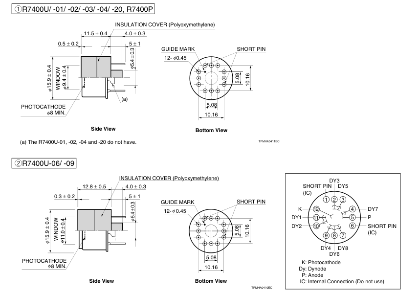
(a): See figure 11. (b): Averaged over any interval of 30 seconds maximum. (c): Measured at 254 nm. (d): Measured after 30 minutes storage in darkness. (e): Measured at 410 nm, at -800 V, with an input pulse width less than 30 ps. (f): Measured at a gain of 106.
Figure 1: Typical Spectral Response (Cs-Te)
WAVELENGTH (nm)
Figure 3: Typical Spectral Response (Multialkali)
WAVELENGTH (nm)
Figure 2: Typical Spectral Response (Bialkali)
WAVELENGTH (nm)
Page 3
| Anode to Cathode Supply Voltage (V) | Anode Characteristics | Type No. | ||||||||
|---|---|---|---|---|---|---|---|---|---|---|
| Anode Sensitivity | Gain Typ. | Anode Dark Current (d) | Time Response | |||||||
| Luminous | Radiant Typ. (A/W) | Typ. (nA) | Max. (nA) | RiseTime Typ. (ns) | Transit Time Typ. (ns) | Transit Time (e) Spread (T.T.S.) (ns) | ||||
| Min. (A/lm) | Typ. (A/lm) | |||||||||
| 800 | — | — | 1100(c) | 5 × 10⁴ | 0.025 | 0.5 | 0.78 | 5.4 | 0.23 | R7400U-09 |
| 800 | 10 | 50 | 4.3 × 10⁴ | 7 × 10⁵ | 0.2 | 2 | 0.78 | 5.4 | 0.23 | R7400U |
| 800 | 10 | 50 | 4.3 × 10⁴ | 7 × 10⁵ | 0.2 | 2 | 0.78 | 5.4 | 0.23 | R7400U-03 |
| 800 | 10 | 50 | 4.3 × 10⁴ | 7 × 10⁵ | 0.2 | 2 | 0.78 | 5.4 | 0.23 | R7400U-06 |
| 800 | 15 | 75 | 3.0 × 10⁴ | 5 × 10⁵ | 0.4 | 4 | 0.78 | 5.4 | 0.23 | R7400U-01 |
| 800 | 25 | 125 | 2.9 × 10⁴ | 5 × 10⁵ | 2 | 20 | 0.78 | 5.4 | 0.23 | R7400U-02 |
| 800 | 35 | 250 | 3.9 × 10⁴ | 5 × 10⁵ | 2 | 20 | 0.78 | 5.4 | 0.23 | R7400U-20 |
| 800 | 15 | 75 | 3.0 × 10⁴ | 5 × 10⁵ | 0.4 | 4 | 0.78 | 5.4 | 0.23 | R7400U-04 |
| 800 | 10 | 50 | 4.3 × 10⁴ | 7 × 10⁵ | 0.2 | 2 | 0.78 | 5.4 | 0.23 | R7401 |
| 800 | 15 | 75 | 3.0 × 10⁴ | 5 × 10⁵ | 0.4 | 4 | 0.78 | 5.4 | 0.23 | R7402 |
| 800 | 25 | 125 | 2.9 × 10⁴ | 5 × 10⁵ | 2 | 20 | 0.78 | 5.4 | 0.23 | R7402-02 |
| 800 | 35 | 250 | 3.9 × 10⁴ | 5 × 10⁵ | 2 | 20 | 0.78 | 5.4 | 0.23 | R7402-20 |
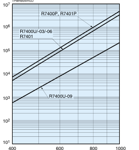
Figure 4: Typical Gain Characteristics
SUPPLY VOLTAGE (V)
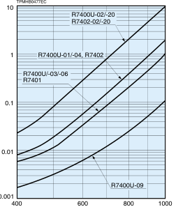
Figure 6: Anode Dark Current (v.s. Supply Voltage)
SUPPLY VOLTAGE (V)
| For Photon Counting (P Type) | ||||
|---|---|---|---|---|
| Type No. | Gain | Dark Count (f) (s-1) | ||
| Min. | Typ. | Typ. | Max. | |
| R7400P | 7.5 × 10⁵ | 1 × 10⁶ | 80 | 400 |
| R7401P | 7.5 × 10⁵ | 1 × 10⁶ | 80 | 400 |
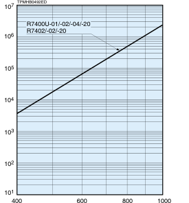
Figure 5: Typical Gain Characteristics
SUPPLY VOLTAGE (V)
Figure 7: Anode Dark Current (v.s. Temperature)
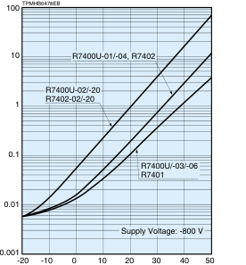
TEMPERATURE (°C)
Page 4
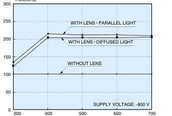
Figure 9: Lens Effect
Figure 8: Transmittance of Lens
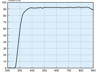
WAVELENGTH (nm)
Figure 10: Lens Effect
R7401
R7402
TPMHB0461EB
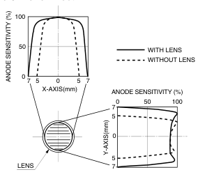
MEASUREMENT CONDITIONS WAVELENGTH : 400 nm SUPPLY VOLTAGE : -800 V A 1 mm diameter spot light (parallel light) is scanned at the center of the photocathode in X and Y directions.
TPMHC0153EB
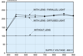
WAVELENGTH (nm)
WAVELENGTH (nm)
Parallel light : Parallel light from a 40 mm diameter parallel light source insuring uniform intensity over the entire active area of the photomultiplier tube.
Diffused light: Diffused light from a 40 mm diameter parallel light source and a diffuser placed 10cm from the detector. The entire active area of the PMT is exposed.
Page 5
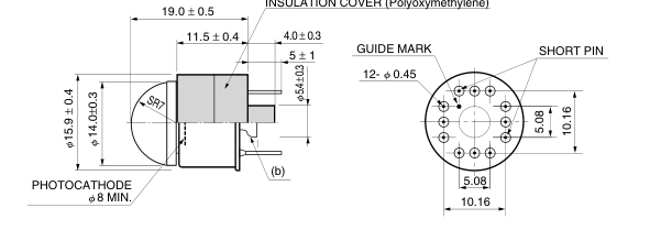
Figure 11: Dimensional Outline and Basing Diagram (Unit: mm)
3R7401, R7401P, R7402/ -02/ -20
INSULATION COVER (Polyoxymethylene)
Side View
Bottom View
TPMHA0415EC
(b) The R7402, -02, and -20 do not have.
Page 6
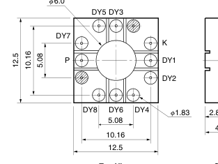
ACCESSORIES (Unit: mm) SOLD SEPARATELY
Socket E678-12M
6.0
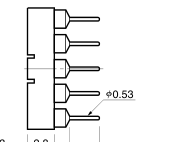
4.2 3.2
Top View
Side View
TACCA0059ED
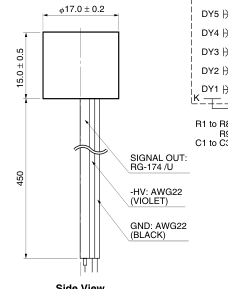
D Type Socket Assemblies E5770/E5780
These are current-output type, small socket assemblies with an internal voltage divider circuit, specifically de- signed for use with the R7400U series.
| Type No. | Grounded Electrode | Divider Resistance (Total) | Maximum Linear Output of Photomultiplier Tube (DC Mode) | Operating Ambient Temperature(c)T | Storage emperature(c) | Output Signal | |
|---|---|---|---|---|---|---|---|
| Cathode Grounded | Anode Grounded | ||||||
| E5770(a) | Anode/Cathode | 2.8 MΩ | 13 µA | 0 °C to +50 °C - | 15 °C to +60 °C | Pulse | DC/Pulse |
| E5780(b) | Anode | — | DC/Pulse | ||||
(a): When operating the E5770 with the cathode grounded (positive high voltage applied to the anode), use a high-voltage resistant capacitor to isolate the signal from the positive high voltage. (b): The E5780 must be operated with the anode grounded (negative high voltage applied to the cathode). If you need a variant type operating with the cathode grounded (positive high voltage applied to the anode), then consult with our sales office. (c): No condensation
Cable Output Type E5780
PC-board Mounting Type E5770
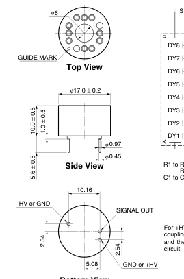
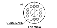
SIGNAL OUT
SIGNAL OUT RG-174/U
GND or +HV R9 C3
GND: AWG22 (BLACK)
P R9 C3
C2 R8
DY8 C2 R8
C1 R7
DY7 C1 R7
R6
DY6
R6
R5
R5
R4
R4
R3
R3
R2
R2
R1 -HV or GND
R1 -HV: AWG22
: 330 kΩ
(VIOLET) : 330 kΩ
R9 : 160 kΩ
: 160 kΩ
: 0.01 µF/ 200 V
: 0.01 µF /200 V
For +HV, it will be necessary to use a coupling capacitor between the output and the customer's signal processing
Bottom View
Side View
TACCA0057EG
TACCA0060EF
Page 7
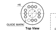
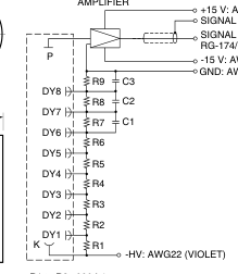
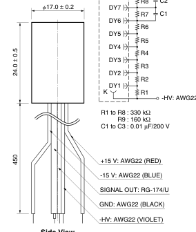
DA Type Socket Assembly C5781
The C5781 is a subminiature socket assembly that incorporates a voltage divider circuit and a low-noise amplifier.
SPECIFICATIONS of Built-in Amplifier
| Parameter | Value | Unit | |
|---|---|---|---|
| Input Voltage for Amplifier | ±15 | V | |
| Current to Voltage Conversion Factor | 1 | V/µA | |
| Maximum Output Voltage (with no load resistor) | 10 | V | |
| Bandwidth (-3 db) | Typ. | DC to 20 | kHz |
| Operating Ambient Temperature (a) | 0 to +40 | °C | |
| Storage Temperature (a) | -15 to +60 | °C | |
(a): No condensation
+15 V: AWG22 (RED) SIGNAL GND SIGNAL OUT
-15 V: AWG22 (BLUE) GND: AWG22 (BLACK)
Side View
TACCA0061ED
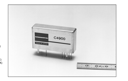
Compact High Voltage Power Supply Units C4900 Series
The C4900 series is an on-board type high voltage power supply unit, with a design that aims at providing both “compactness and high performance”. The newly developed circuit achieves high performance
and low power consumption. The C4900 series in addition provides enhanced protective functions yet is offered at lower costs.
SPECIFICATIONS
| Parameter | C4900 | C4900-01 | C4900-50 | C4900-51 | |
|---|---|---|---|---|---|
| Input Voltage | +15 V | +12 V | +15 V | +12 V | |
| Input Current (a) | 1 | 14 mA | 15 mA | 14 mA | 15 mA |
| 2 | 90 mA | 95 mA | 90 mA | 95 mA | |
| Variable Output Range | 0 V to -1250 V | 0 V to +1250 V | |||
| Maximum Output Current | 0.6 mA | 0.5 mA | 0.6 mA | 0.5 mA | |
| Ripple Noise (p-p) | 0.007 % Typ. | ||||
| Line Regulation (b) | ±0.01 % Typ. | ||||
| Load Regulation (c) | ±0.01 % Typ. | ||||
| Operating Ambient Temperature (d) | 0 °C to +50 °C | ||||
| Storage Temperature | -20 °C to +70 °C | ||||
| Dimension (e) (W×H×D) | 46 mm × 24 mm × 12 mm | ||||
1With No Load 2With Full Load (a): At Maximum Output Voltage. (b): Against ±1 V Change. (c): Against 0 to 100 % Load Change. (d): At Maximum Output Voltage and Current. (e): Excluding Projecting Parts
Page 8
WARNING: HIGH VOLTAGE

RELATED PRODUCTS
\*PATENT: USA: 5410211 and other(9), GBR: 551767 and other(9), DEU: 69209809 and other(9), FRA: 551767 and other(9), JPN: 3078905 and other(9)
WEB SITE http://www.hamamatsu.com
HAMAMATSU PHOTONICS K.K., Electron Tube Division 314-5, Shimokanzo, Toyooka-village, Iwata-gun, Shizuoka-ken, 438-0193, Japan, Telephone: (81)539/62-5248, Fax: (81)539/62-2205 U.S.A.: Hamamatsu Corporation: 360 Foothill Road, P. O. Box 6910, Bridgewater. N.J. 08807-0910, U.S.A., Telephone: (1)908-231-0960, Fax: (1)908-231-1218 E-mail: usa@hamamatsu.com Germany: Hamamatsu Photonics Deutschland GmbH: Arzbergerstr. 10, D-82211 Herrsching am Ammersee, Germany, Telephone: (49)8152-375-0, Fax: (49)8152-2658 E-mail: info@hamamatsu.de France: Hamamatsu Photonics France S.A.R.L.: 8, Rue du Saule Trapu, Parc du Moulin de Massy, 91882 Massy Cedex, France, Telephone: (33)1 69 53 71 00, Fax: (33)1 69 53 71 10 E-mail: infos@hamamatsu.fr
United Kingdom: Hamamatsu Photonics UK Limited: 2 Howard Court, 10 Tewin Road Welwyn Garden City Hertfordshire AL7 1BW, United Kingdom, Telephone: 44-(0)1707-294888, Fax: 44(0)1707-325777 E-mail: info@hamamatsu.co.uk North Europe: Hamamatsu Photonics Norden AB: Smidesvägen 12, SE-171-41 SOLNA, Sweden, Telephone: (46)8-509-031-00, Fax: (46)8-509-031-01 E-mail: info@hamamatsu.se
TPMH1204E07
Italy: Hamamatsu Photonics Italia: S.R.L.: Strada della Moia, 1/E, 20020 Arese, (Milano), Italy, Telephone: (39)02-935 81 733, Fax: (39)02-935 81 741 E-mail: info@hamamatsu.it
MAY 2004 IP (1000)