

 Download PDF
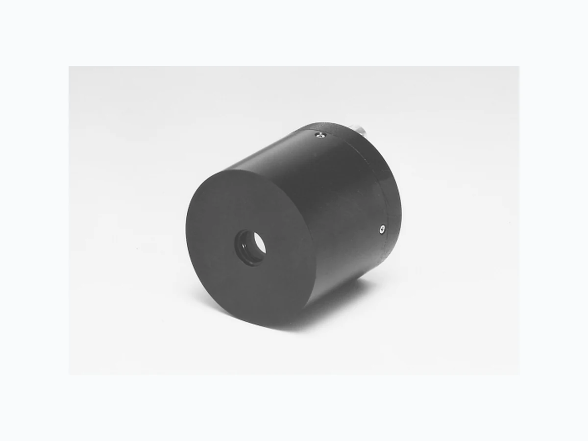
R5916U-50 HAMAMATSU
Document overview
- PDF pages: 8
Technical content
Page 1

Featuring Fast Gating Function with Improved Time Response
and High Switching Ratio
FEATURES
GHigh Speed Gating by Low Supply Voltage (+10 V)
Gate Rise Time : 1 ns A Gate Width : 5 ns
GFast Rise Time : 180 ps
Narrow TTS B : 90 ps
GHigh Switching Ratio: 108 at 500 nm GLow Switching Noise GLow Dark Noise GVariety of Photocathode Available
APPLICATIONS
GEnvironmental monitoring GSatellite laser ranging GTime resolve fluorescence decay analysis
Figure 1: Typical Anode Output Waveform
TPMHB0245EB
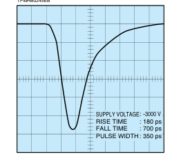
TIME (0.2 ns/div)
Figure 2: Block Diagram of Anode Output Waveform Measuring Apparatus
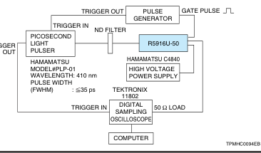
TRIGGER
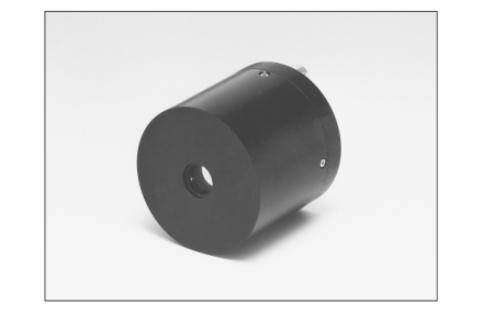
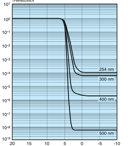
Figure 3: Typical Gate Bias Characteristics (R5916U-50)
TPMHB0244EA
INPUT GATE BIAS VOLTAGE (V)
These are the anode output ratios measured at the forward and reverse bias voltages with respect to the photocathode.
Subject to local technical requirements and regulations, availability of products included in this promotional material may vary. Please consult with our sales office. Information furnished by HAMAMATSU is believed to be reliable. However, no responsibility is assumed for possible inaccuracies or omissions. Specifications are subject to change without notice. No patent rights are granted to any of the circuits described herein. ©2007 Hamamatsu Photonics K.K.
Page 2
SPECIFICATIONS
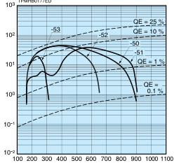
PHOTOCATHODE SELECTION GUIDE
| Suffix Number | Spectral Response (nm) | Photocathode Material | Photocathode Window Material | |
| Range | Peak Wavelength | |||
| 50 | 160 to 850 | 430 | Multialkali | Synthetic Silica |
| 51 | 160 to 910 | 600 | Extended Red Multialkali | Synthetic Silica |
| 52 | 160 to 650 | 400 | Bialkali | Synthetic Silica |
| 53 | 160 to 320 | 250 | Cs-Te | Synthetic Silica |
GENERAL CHARACTERISTICS
| Parameter | Description / Value | Unit |
|---|---|---|
| Photocathode Effective Area in Diameter | 10 | mm |
| MCP Channel Diameter | 6 | µm |
| Dynode Structure C | 2-Stage Filmed MCP | — |
| Capacitance between Mesh Electrode and Photocathode | 14.7 | pF |
| Operating Ambient Temperature | -50 to +50 | °C |
| Storage Temperature | -50 to +50 | °C |
MAXIMUM RATINGS (Absolute Maximum Values)
| Parameter | Value | Unit |
|---|---|---|
| Supply Voltage | -3400 | V |
| Average Anode Current | 100 | nA |
| Pulse Peak Current D | 350 | mA |
ELECTRICAL CHATACTERISTICS (R5916U-50) at 25 °C E
| Parameter | Min. | Typ. | Max. | Unit | |
|---|---|---|---|---|---|
| Cathode Sensitivity | Luminous F | 100 | 150 | — | µA/lm |
| Radiant at 430 nm | — | 50 | — | mA/W | |
| Gain (at -3000 V) | 1 × 10⁵ | 2 × 10⁵ | — | — | |
| Anode Dark Counts (at -3000 V) G | — | 10 | — | s-1 | |
| Voltage Divider Current | — | — | 100 | µA | |
| Switching Ratio (at 500 nm) | — | 1.7 × 10⁸ | — | — | |
| Time Response (at -3000 V) | Rise Time H | — | 180 | — | ps |
| Fall Time I | — | 700 | 1000 | ps | |
| IRF (FWHM) J | — | 95 K | — | ps | |
| TTS (FWHM) | — | 90 L | — | ps | |
GATING CHARACTERISTICS
| Parameter | Min. | Typ. | Max. | Unit | |
|---|---|---|---|---|---|
| Input Gate Pulse | Voltage | 10 | — | 50 | V |
| Width | 5 | — | 10 000 | ns | |
| Duty Cycle | — | — | 1 | % | |
| PMT response | Rise Time | — | 1 | — | ns |
| Fall Time | — | 1 | — | ns | |
Page 3
NOTES
A This is defined at 10 % to 90 % of full pulse height. B Transit time spread (TTS) is the fluctuation in transit time among individual pulses and specified as an FWHM (full width at half maximum) with the incident light having a single photoelectron state. C Two microchannel plates (MCPs) are incorporated as a standard but we can provide it with either one or three MCPs as an option depending upon your request. D This is specified under the operating conditions that the repetition rate of light input is 100 Hz or less and its pulse width is 70 ps or less. E This is based on R5916U-50. All other types (suffix number 51, 52 and 53) have different characteristics based on photocathode sensitivity and anode dark
counts. F The light source used to measure the luminous sensitivity is a tungsten filament lamp operated at a distribution temperature of 2856 K. The incident light intensity is 10-4 lumen and 200 V is applied between photocathode and all other electrodes shorted as an anode. G This is specified at a duty cyde of 1 %. H This is the mean time difference between the 10 % and 90 % amplitude points on the output waveform under full photocathode illumination. I This is the mean time difference between the 90 % and 10 % amplitude points on the tailing edge of the output waveform under full photocathode illumination. J IRF stands for Instrument Response Function which is a convolution of the δ-function (H(t)) of the measuring apparatus and the exciation function (E(t)) of a
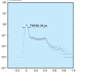
laser. The IRF is given by the following formula: IRF = H(t)∗ E(t) K We specity the IRF as an FWHM of the time distribution taken by using the measuring apparatus in Figure 7 that is Hamamatsu standard IRF measuring setup. It can be estimated by the following equation: (IRF (FWHM))2 = (TTS)2 + (Tw)2 + (Tj)2 where Tw is the pulse width of the laser and Tj is the time jitter of all equipments used in the measurement. An IRF is provided with the tube. L TTS stands for Transit Time Spread (see B). Assuming that the laser pulse width (Tw) and time jitter of all equipment (Tj) used in Figure 7 are negligible, IRF can be estimated as equal to TTS (see B). Therefore, the TTS can be estimated to be 90 ps or so.
INPUT GATE PULSE
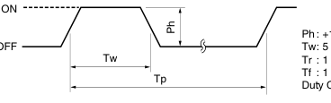
GATE ON
GATE OFF
PMT OPERATING MODE
Tw
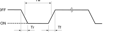
: +10 V to +50 V : 5 ns to 10 µs : 1 ns (10 % to 90 %) : 1 ns (90 % to 10 %)
<=
Duty Cycle: Tw/Tp 0.01
TACCC0044EA
R5916U-50 will be provided in a "normally off" mode configuration. It will be gated "on" only when the gate input pulse (+10 V to +50 V)
is applied and gated "off" when it is grounded or left in open.
However, we can also provide this device in a "normally on" mode configuration which can be operated under the same operating conditions above to give inverse performance. Please specify if you require a "normally on" mode configuration when placing an order.
TYPICAL PERFORMANCE DATA
Figure 5: Instrument Response Function (IRF)
Figure 4: Spectral Response Characteristics
TPMHB0246EB
TPMHB0177ED
TIME (ns)
WAVELENGTH (nm)
Page 4
Figure 6: Gain
TPMHB0179EA
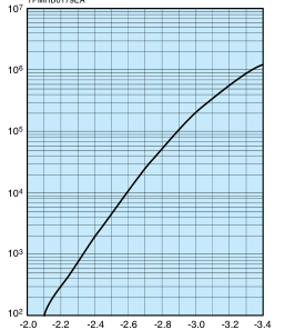
SUPPLY VOLTAGE (kV)
Figure 8: Pulse Height Distribution (PHD)
TPMHB0337EB
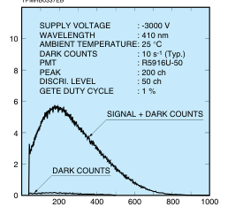
PULSE HEIGHT (CHANNEL NUMBER)
Figure 10: Gate Pulse Response
TPMHB0338EA
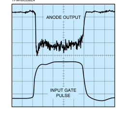
5 ns/div Supply Voltage
: -3000 V
Wavelength
: 410 nm
Ambient Temperature: 25 °C Gate Pulse Height : 10 V Gate Pulse Width : 25 ns Repetition Rate
: 1 kHz
Figure 7: Block Diagram of IRF (Instrument Response Function) Measuring Apparatus
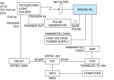
HAMAMATSU MODEL#PLP-01 WAVELENGTH: 410 nm PULSE WIDTH (FWHM) : 35 ps
TPMHC0095EB
Figure 9: Block Diagram of PHD Measuring Apparatus
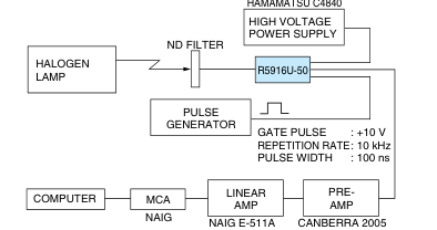
TPMHC0102EA
Figure 11: Block Diagram of Gate Pulse Response Measuring Apparatus
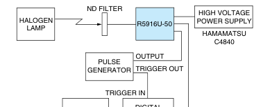
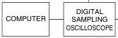
50 Ω LOAD
TPMHC0103EA
Page 5
Figure 12: Dimensional Outline (Umit: mm)
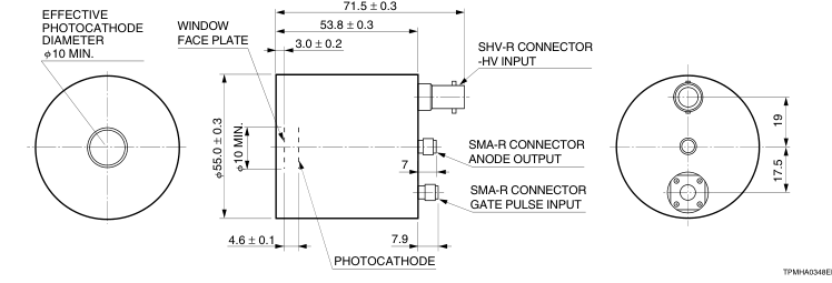
Figure 13: Voltage Divider and Gate Circuit
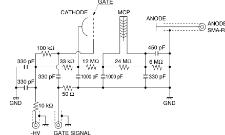
ANODE OUTPUT
SHV-R INPUT SMA-R Some of the values indicated in this circuit may be different from actual values to meet the specifications.
TPMHC0090EC
FUNDAMENTAL OPERATING PROCEDURE
1) A general set-up for R5916U-50 is shown at right.
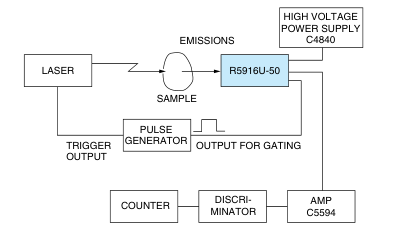
This is to perform a photon counting with gating function and to detect weak light generated from the samples by the laser excitation.
2) The pulse generator used in this set-up produce an output
having +10 V in height and adjustable width which you re- quire. It also produces a trigger signal synchronyzing an output pulse to the laser output. The R5916U-50 is in gate
off mode in the beginning to prevent unwanted signals caused by the laser light or some scattered light which may strike the photocathode directly.
3) The pulse generator required for gating function is very
simple. The required specifications for the pulse generator is as follows:
TPMHC0096EA
a. Output voltage is +10 V to +15 V. b. Pulse width is just what you require (between 5 ns and
10 ms).
Page 6
EXAMPLE OF APPLICATIONS
ENVIRONMENTAL MONITORING
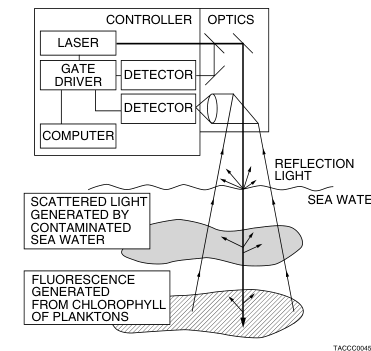
This is an example of laser radar (LIDAR) application where our gateable MCP-PMT has been used. The sketch at right shows a LIDAR system which includes a picosecond laser, electronics (gate driver), optics, computer and sensor (gateable MCP-PMT). This system is to investigate the distribution of planktons in the ocean for pollution monitoring. The laser light irradiates sea water and generates some scattered light due to contaminated water and fluorescence due to chlorophyll in planktons. By detecting these emissions, a distribution of quantative and qualitative informations on these objects can be obtained. However, there are enormous back ground emissions due to reflections of
the laser light off of the water's surface as well as from particles in an air or some unknown materials in the ocean. Sun light is also a source of back ground if the ex- periment has to be performed in day time. In this application, fast gating function is very effective to minimize the back ground noise. The tube is gated on only during the time when essence emissions arrive at the de- tector. The switching ratio characteristics are also very important to help minimize the noise. The R5916U-50 series tubes are superior on both characteristics.
SATELLITE LASER RANGING (SLR)
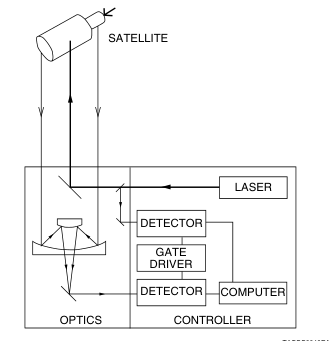
This is also an example of a LIDAR application where the gateable MCP-PMT has been used to measure the distance between the observatory and a satellite. The operating principle is that a satellite is irradiated by the fast laser pulse and then a reflected light is directed to the detector through the optics placed on the ground. The time interval of the signals from the source to the detector in the system is the time of flight (TOF) from the observatory to the satellite and can be converted into a distance between them. This entire system consists of fast laser, optics, electronics, gate driver and detectors. The data taken by experiments with this system are also utilized for geodesy or
plate motion analysis on a world-wide level. Because of the improved timing characteristics with R5916U-50 series, more precise measurements can be expected.
References
Laser Radar (LIDAR) system a)
Laser Satellite Ranging system b)
TACCC0046EA
a) Japan Marine Science and Technology Center: R&D of Laser Ranging Technology (Published in Japan) b) HITACHI: Laser Satellite Ranging System
Page 7
PRECAUTIONS FOR PROPER OPERATION
- The photomultiplier tube (PMT) in this data sheet is a glass product under high vacuum. Excessive pressure or shocks to the tube from the surroundings could cause a permanent damage. Please pay special attention on insuring proper handling. 2. Do not expose the photocathode to direct sunlight and any light stronger than the room light even during of no operation. 3. Do not supply any voltage higher than specified. Also make sure the output current does not exceed the maximum current specified. 4. This device is very sensitive even with weak light input. When applying high voltage to the tube, gradually (ideally 100 V step) and carefully increase the voltage while monitoring the output using a current meter or oscilloscope (if the PMT has multianodes,
please make all the anode summed when monitoring). Also make sure before use that the polarity of the applied voltage is correct. 5. Never touch the input window with your bare hands. In case the window contaminated by dust or grease, wipe it off using alcohol and a soft cloth or dust free tissue. 6. Do not remove any input or output cables when high voltage is applied. 7. Do not place any objects of ground potential closer than 5 mm to the photocathode window when negative high voltage is applied to the photocathode. It could generate extra noise and damage the photocathode permanently. 8. Do not operate or store in a place of unspecified temperature and humidity.
- If the tube won't be used with a cooler, it is recommended to leave the tube in darkness (your instrument without any input light) for 30 minutes or so before start any measurements because it occasionally takes a little while until its dark noise settles down.
WARRANTY
The detectors indicated in this data sheet are warranted to the original purchaser for a period of 12 months following the date of shipment. The warranty is limited to repair or replacement of any defective material due to defects in workmanship or materials used in manufacture.
- Any claim for damage of shipment must be made directly to the delivering carrier within five days. 2. Customer must inspect and test all detectors within 30 days after shipment. Failure to accomplish said incoming inspection shall limit all claims to 75 % of invoice value. 3. NO credit will be issued for broken detector unless in the opinion of Hamamatsu the damage is due to a manufacturing defect. 4. NO credit will be issued for any detector which in the judgement of Hamamatsu has been damaged, abused, modified or whose serial number or type number have been obliterated or defaced. 5. NO detector will be accepted for return unless permission has been obtained from Hamamatsu in writing, the shipment has been
returned repaired and insured, the detector is packed in their original box and accompanied by the original data sheet furnished to the customer with the tube, and a full written explanation of the reason for rejection of detector.
Page 8
ACCESSORIES
HIGH SPEED AMPLIFIER C5594 Series
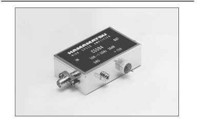
Suffix numbers and input / output connectors
| Input Connectors | Output Connectors | |
| SMA Jack | BNC Jack | |
| SMA Plug (male) | C5594-12 | C5594-14 |
| SMA Receptacle (female) | C5594-22 | C5594-24 |
| BNC Plug (male) | C5594-32 | C5594-34 |
| BNC Receptacle (female) | C5594-42 | C5594-44 |
Specifications
| Parameters | Description / Value | ||
|---|---|---|---|
| Frequency Response Range | 50 kHz to 1.5 GHz | ||
| Gain | Typ. | 36 dB | |
| Input / Output Impedance | 50 Ω | ||
| Noise Figure (NF) | Typ. | 5 dB | |
| Recommend Input Voltage | +12 V to 16 V | ||
| Supply Current | Typ. | 95 mA | |
| Absolute Maximum Ratings | Supply Voltage | +17 V | |
| Input Power | +10 mW | ||
BENCH-TOP HIGH VOLTAGE POWER SUPPLY C4840 Series
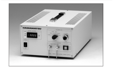
Specifications
| Parameter | Description / Value | ||
|---|---|---|---|
| Output Voltage | 0 V to ±3000 V | ||
| Maximum Output Current | 10 mA | ||
| Line Regulation Against ±10 % Line Voltage Change AB | Max. | ±(0.005 % + 10 mV) | |
| Load Regulation Against 0 % to 100 % Load Change A | Max. | ±(0.01 % + 50 mV) | |
| Ripple / Noise (p-p) AB | Max. | 0.0007 % | |
| Drift (after 1 h Warm-up) AB | Max. | ±(0.02 % + 10 mV)/8 h | |
| Temperature Coefficient AB | Max. | ±0.01 % / °C | |
| AC Input Voltage | C4840-01 | 120 V (±10 %) (50 / 60 Hz) | |
| C4840-02 | 230 V (±10 %) (50 / 60 Hz) | ||
| Power Consumption AB | Approx. 100 V·A | ||
| Operating Ambient Temperature / Humidity C | 0 °C to +40 °C / below 80 % | ||
| Storage Temperature / Humidity C | -20 °C to +50 °C / below 85 % | ||
NOTE: AAt maximum output voltage BAt maximum output current CNo condensation
WEB SITE www.hamamatsu.com
HAMAMATSU PHOTONICS K.K., Electron Tube Division 314-5, Shimokanzo, Iwata City, Shizuoka Pref., 438-0193, Japan, Telephone: (81)539/62-5248, Fax: (81)539/62-2205 U.S.A.: Hamamatsu Corporation: 360 Foothill Road, P. O. Box 6910, Bridgewater. N.J. 08807-0910, U.S.A., Telephone: (1)908-231-0960, Fax: (1)908-231-1218 E-mail: usa@hamamatsu.com Germany: Hamamatsu Photonics Deutschland GmbH: Arzbergerstr. 10, D-82211 Herrsching am Ammersee, Germany, Telephone: (49)8152-375-0, Fax: (49)8152-2658 E-mail: info@hamamatsu.de France: Hamamatsu Photonics France S.A.R.L.: 19, Rue du Saule Trapu, Parc du Moulin de Massy, 91882 Massy Cedex, France, Telephone: (33)1 69 53 71 00, Fax: (33)1 69 53 71 10 E-mail: infos@hamamatsu.fr
United Kingdom: Hamamatsu Photonics UK Limited: 2 Howard Court, 10 Tewin Road Welwyn Garden City Hertfordshire AL7 1BW, United Kingdom, Telephone: 44-(0)1707-294888, Fax: 44(0)1707-325777 E-mail: info@hamamatsu.co.uk North Europe: Hamamatsu Photonics Norden AB: Smidesvägen 12, SE-171-41 SOLNA, Sweden, Telephone: (46)8-509-031-00, Fax: (46)8-509-031-01 E-mail: info@hamamatsu.se
TPMH1102E06
Italy: Hamamatsu Photonics Italia: S.R.L.: Strada della Moia, 1/E, 20020 Arese, (Milano), Italy, Telephone: (39)02-935 81 733, Fax: (39)02-935 81 741 E-mail: info@hamamatsu.it
AUG. 2007 IP