


 Download PDF
R5611 HAMAMATSU
Document overview
- PDF pages: 4
Technical content
Page 1
PHOTOMULTlPLlER TUBES
R5611, R5611–01
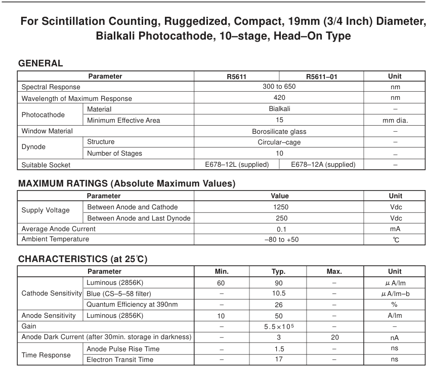
| Parameter | R5611 | R5611–01 | Unit | |
|---|---|---|---|---|
| Spectral Response | 300 to 650 | nm | ||
| Wavelength of Maximum Response | 420 | nm | ||
| Photocathode | MateriaI | Bialkali | ||
| Minimum Effective Area | 15 | mm dia. | ||
| Window MateriaI | Borosilicate glass | |||
| Dynode | Structure | Circular–cage | ||
| Number of Stages | 10 | |||
| SuitabIe Socket | E678–12L (supplied) | E678–12A (supplied) | ||
| Parameter | Value | Unit | |
|---|---|---|---|
| Supply Voltage | Between Anode and Cathode | 1250 | Vdc |
| Between Anode and Last Dynode | 250 | Vdc | |
| Average Anode Current | 0.1 | mA | |
| Ambient Temperature | –80 to +50 | ||
NOTE: Anode characteristics are measured with the voItage distribution ratio shown below.
VOLTAGE DlSTRlBUTlON RATlO AND SUPPLY VOLTAGE
K Dy1 Dy2 Dy3 Dy4 Dy5
Dy6 Dy7
Dy8 Dy9 Dy10
P
Electrodes Ratio
3 1 1 1 1 1 1 1 1 1 1
SuppIy Voltage : 1000Vdc, K : Cathode, Dy : Dynode, P : Anode
ENVIRONMENTAL TESTING
. . . . . . . . . . . . . . . . . . . . . . . . . . . . . . . .
100g's, 11 1ms, 3 impact shocks per direction (6 directions)
Shoch . . . . . . . . . . . . . . . . . . . . . . . . . . .
20g's, 50 to 2000Hz, 1 oct per minute, 3 sweeps per axis (3 axes)
Vibration
Subject to local technical requirements and regulations, availability of products included in this promotional material may vary. Please consult with our sales office. lnformation furnished by HAMAMATSU is believed to be reliabIe. However, no responsibility is assumed for possibIe inaccuracies or commission. Specifications are subjected to change without notice. No patent right are granted to any of the circuits described herein. © 1994 Hamamatsu Photonics K.K.
Page 2
PHOTOMULTlPLlER TUBES R5611, R5611–01
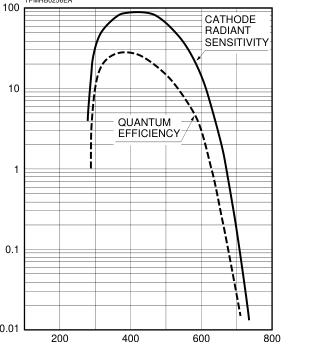
Figure 1: Typical Spectral Response
TPMHB0256EA
WAVELENGTH (nm)
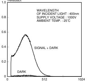
Figure 3: Single Photoelectron Pulse Height Distribution
CHANNEL NUMBER (CH)
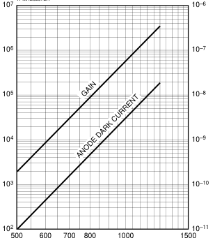
Figure 2: Typical Gain and Dark Current
TPMHB0267EA
SUPPLY VOLTAGE (V)
Figure 4: Temperature Coefficient of Anode Sensitivity
TPMHB0269EA
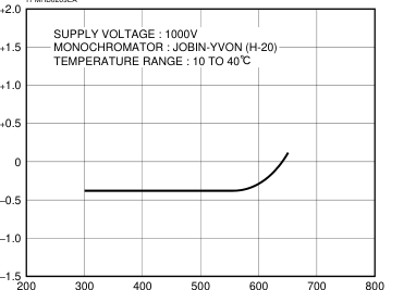
WAVELENGTH (nm)
Page 3
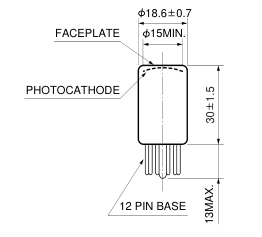
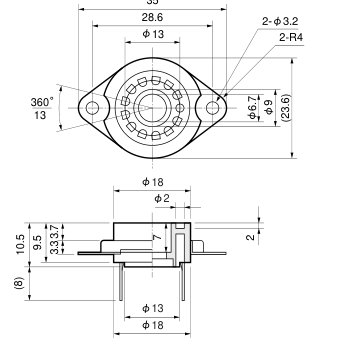
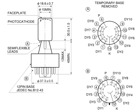
Figure 5: R5611 Dimensional Outline and Basing Diagram (Unit : mm)
Socket
(E678–12L) 35
K DY1
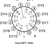
SHORT PIN
TPMHA0269EA
TACCA0047EA
Figure 6: R5611-01 Dimensional Outline and Basing Diagram (Unit : mm)
Socket
(E678–12A)
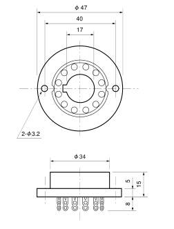
TPMHA0270EB
TACCA0009EB
Page 4
PHOTOMULTlPLlER TUBES R5611, R5611–01
HAMAMATSU PHOTONICS K.K., Electoron Tube Center 314-5, Shimokanzo, Toyooka-village, Iwata-gun, Shizuoka-ken, 438-0193, Japan, Telephone: (81)539/62-5248, Fax: (81)539/62-2205 U.S.A.: Hamamatsu Corporation: 360 Foothill Road, Bridgewater. N.J. 08807-0910, U.S.A., Telephone: (1)908-231-0960, Fax: (1)908-231-1218 Germany: Hamamatsu Photonics Deutschland GmbH: Arzbergerstr. 10, D-82211 Herrsching am Ammersee, Germany, Telephone: (49)8152-375-0, Fax: (49)8152-2658 France: Hamamatsu Photonics France S.A.R.L.: 8, Rue du Saule Trapu, Parc du Moulin de Massy, 91882 Massy Cedex, France, Telephone: (33)1 69 53 71 00, Fax: (33)1 69 53 71 10 United Kingdom: Hamamatsu Photonics UK Limted: Lough Point, 2 Gladbeck Way, Windmill Hill, Enfield, Middlesex EN2 7JA, United Kingdom, Telephone: (44)181-367-3560, Fax: (44)181-367-6384
TPMH1108E02
North Europe: Hamamatsu Photonics Norden AB: Färögatan 7, S-164-40 Kista Sweden, Telephone: (46)8-703-29-50, Fax: (46)8-750-58-95 Italy: Hamamatsu Photonics Italia: S.R.L.: Via Della Moia, 1/E, 20020 Arese, (Milano), Italy, Telephone: (39)2-935 81 733, Fax: (39)2-935 81 741
JAN. 1995