

 Download PDF
R446 HAMAMATSU
Document overview
- PDF pages: 4
Technical content
Page 1

Multialkali Photocathode Sensitive to 870 nm
28 mm (1-1/8 Inch) Diameter, 9-Stage, Side-On Type
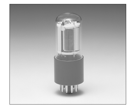
The R446 features high quantum efficiency, high current amplification, good S/N ratio and wide spectral response from UV to near infrared. The R446 employs a UV-transmitting glass envelope for UV sensitivity extension. The R446 is well suited for use in broad-band spectrophotometers, atomic absorption spectrophotometers, chromatographs, NOx analyzers and other precision photometric instruments.
FEATURES
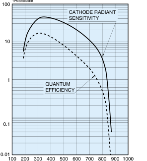
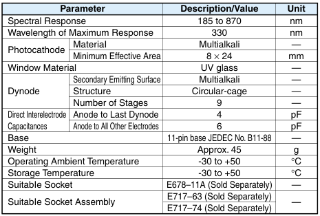
GWide Spectral Response ......................... 185 nm to 870 nm GCathode Sensitivity Luminous ......................................................... 120 µA/lm Radiant at 330 nm ............................................. 44 mA/W GAnode Sensitivity (at 1000 V) Luminous ........................................................... 600 A/lm Radiant at 330 nm ...................................... 2.2 × 10⁵ A/W GLow Drift and Hysteresis
Figure 1: Typical Spectral Response
SPECIFICATIONS
GENERAL
WAVELENGTH (nm)
Subject to local technical requirements and regulations, availability of products included in this promotional material may vary. Please consult with our sales office. Information furnished by HAMAMATSU is believed to be reliable. However, no responsibility is assumed for possible inaccuracies or omissions. Specifications are subject to change without notice. No patent rights are granted to any of the circuits described herein. ©2006 Hamamatsu Photonics K.K.
Page 2
PHOTOMULTIPLIER TUBES R446
MAXIMUM RATINGS (Absolute Maximum Values)
| Parameter | Value | Unit | |
|---|---|---|---|
| Supply Voltage | Between Anode and Cathode | 1250 | V |
| Between Anode and Last Dynode | 250 | V | |
| Average Anode Current A | 0.1 | mA | |
CHARACTERISTlCS (at 25 °C)
| Parameter | Min. | Typ. | Max. | Unit | ||
|---|---|---|---|---|---|---|
| Cathode Sensitivity | Quantum Efficiency (at Peak Wavelength) | — | 16.7 (at 320 nm) | — | % | |
| Luminous B | 80 | 120 | — | µA/lm | ||
| Radiant | at 194 nm | — | 9.0 | — | mA/W | |
| at 254 nm | — | 25 | — | mA/W | ||
| at 330 nm | — | 44 | — | mA/W | ||
| at 633 nm | — | 17 | — | mA/W | ||
| at 852 nm | — | 0.25 | — | mA/W | ||
| Red/White Ratio C | 0.1 | 0.25 | — | — | ||
| Blue Sensitivity Index D | — | 6.0 | — | — | ||
| Anode Sensitivity | Luminous E | 100 | 600 | — | A/lm | |
| Radiant | at 194 nm | — | 4.5 × 10⁴ | — | A/W | |
| at 254 nm | — | 1.3 × 10⁵ | — | A/W | ||
| at 330 nm | — | 2.2 × 10⁵ | — | A/W | ||
| at 633 nm | — | 8.5 × 10⁴ | — | A/W | ||
| at 852 nm | — | 1.3 × 10³ | — | A/W | ||
| Gain E | — | 5.0 × 10⁶ | — | — | ||
| Anode Dark Current F (After 30 min Storage in Darkness) | — | 3 | 50 | nA | ||
| ENI (Equivalent Noise Input) H | — | 3.1 × 10⁻¹⁶ | — | W | ||
| Time Response E | Anode Pulse Rise Time I | — | 2.2 | — | ns | |
| Electron Transit Time J | — | 22 | — | ns | ||
| Anode Current StabilityK | Light Hysteresis | — | 0.1 | — | % | |
| Voltage Hysteresis | — | 1.0 | — | % | ||
NOTES
A: Averaged over any interval of 30 seconds maximum. B: The light source is a tungsten filament lamp operated at a distribution temperature of 2856K. Supply voltage is 100 V between the cathode and all other electrodes connected together as anode. C:Red/White ratio is the quotient of the cathode current measured using a red filter (Toshiba R-68) interposed between the light source and the tube by the cathode current measured with the filter removed under the same conditions as Note B. D:The value is cathode output current when a blue filter (Corning CS 5-58 polished to 1/2 stock thickness) is interposed between the light source and the tube under the same condition as Note B.
E: Measured with the same light source as Note B and with the voltage distribution ratio shown in Table 1 below.
Table 1:Voltage Distribution Ratio
| Electrode | K | Dy1 | Dy2 | Dy3 | Dy4 | Dy5 | Dy6 | Dy7 | Dy8 | Dy9 | P | |||||||||||
| Distribution Ratio | 1 | 1 | 1 | 1 | 1 | 1 | 1 | 1 | 1 | 1 | ||||||||||||
SuppIy Voltage: 1000 V, K: Cathode, Dy: Dynode, P: Anode
F: Measured with the same supply voltage and voltage distribution ratio as Note E after removal of light. G:Measured at a supply voltage adjusted to provide an anode sensitivity of 100 A/lm. H:ENI is an indication of the photon-limited signal-to-noise ratio. It refers to the amount of light in watts to produce a signal-to-noise ratio of unity in the output of a photomultiplier tube.
2q.ldb.G.∆f ENI = S where q = Electronic charge (1.60 × 10⁻¹⁹ coulomb). ldb = Anode dark current(after 30 minute storage) in amperes. G = Gain. ∆f = Bandwidth of the system in hertz. 1 hertz is used. S = Anode radiant sensitivity in amperes per watt at the wavelength of peak response.
I: The rise time is the time for the output pulse to rise from 10 % to 90 % of the peak amplitude when the entire photocathode is illuminated by a delta function light pulse. J: The electron transit time is the interval between the arrival of delta function light pulse at the entrance window of the tube and the time when the anode output reaches the peak amplitude. In measurement, the whole photocathode is illuminated. K: Hysteresis is temporary instability in anode current after light and voltage are applied.
l max.
il l min. TIME 7 (minutes)
TPMSB0002EA
lmax. lmin.
× 100 (%)
Hysteresis =
li
Page 3
(1)Light Hysteresis The tube is operated at 750 V with an anode current of 1 µA for 5 minutes. The light is then removed from the tube for a minute. The tube is then re-illuminated by the previous light level for a minute to measure the variation.
Figure 2: Anode Luminous Sensitivity and
Gain Characteristics
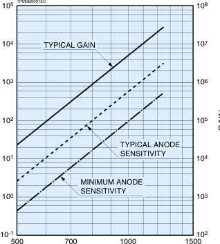
SUPPLY VOLTAGE (V)
Figure 4: Typical Temperature Coefficient of Anode Sensitivity
TPMSB0093EC
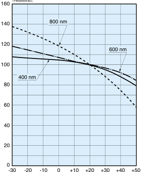
TEMPERATURE (°C)
((2)Voltage Hysteresis The tube is operated at 300 V with an anode current of 0.1 µA for 5 minutes. The light is then removed from the tube and the supply voltage is quickly increased to 800 V. After a minute, the supply voltage is then reduced to the previous value and the tube is re-illuminated for a minute to measure the variation.
Figure 3: Typical Time Response
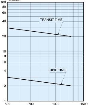
SUPPLY VOLTAGE (V)
Figure 5: Typical Temperature Characteristic of Dark Current (at 1000 V, after 30 min strage in darkness)
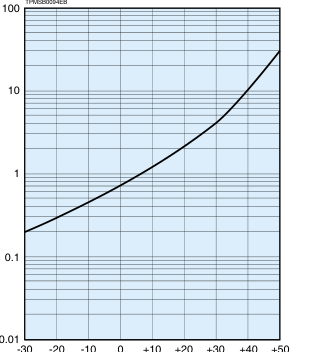
TEMPERATURE (°C)
Page 4
PHOTOMULTIPLIER TUBES R446
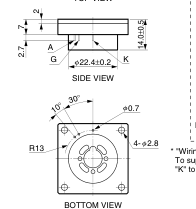
Figure 6: Dimensional Outline and Basing Diagram (Unit: mm)
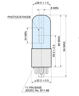
DY6 DY7 DY5 6 5 7
DY4
DY8
4 8
3 DY3
9 DY9
2 10 P
DY2 1 11 K DY1
DIRECTION OF LIGHT
Bottom View
(Basing Diagram)
TPMSA0008EA
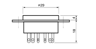
Figure 8: D Type Socket Assembly (Unit: mm) Sold Separately
E717-63
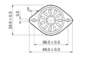
SOCKET
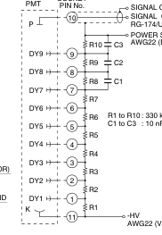
SIGNAL OUTPUT RG-174/U(BLACK) POWER SUPPLY GND AWG22 (BLACK)
29.0 ± 0.3
| 0.7 31.0 ± | 0.5 HOUSING (INSULATOR) POTTING COMPOUND |
AWG22 (VIOLET)
TACCA0002EH
\* Hamamatsu also provides C4900 series compact high voltage power
Figure 7: Socket (Unit: mm) Sold Separately
E678-11A
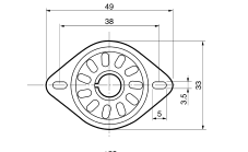
TACCA0064EA
E717-74 HOUSING
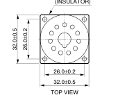
SOCKET PMT
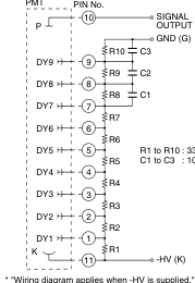
: 330 kΩ : 10 nF
To supply +HV,connect the pin "G" to+HV, and the pin "K" to the GND.
TACCA0277EA
supplies and C6270 series DP type socket assemblies which incor- porate a DC to DC converter type high voltage power supply.
WEB SITE www.hamamatsu.com
HAMAMATSU PHOTONICS K.K., Electron Tube Division 314-5, Shimokanzo, Iwata City, Shizuoka Pref., 438-0193, Japan, Telephone: (81)539/62-5248, Fax: (81)539/62-2205
U.S.A.: Hamamatsu Corporation: 360 Foothill Road, P. O. Box 6910, Bridgewater. N.J. 08807-0910, U.S.A., Telephone: (1)908-231-0960, Fax: (1)908-231-1218 E-mail: usa@hamamatsu.com Germany: Hamamatsu Photonics Deutschland GmbH: Arzbergerstr. 10, D-82211 Herrsching am Ammersee, Germany, Telephone: (49)8152-375-0, Fax: (49)8152-2658 E-mail: info@hamamatsu.de France: Hamamatsu Photonics France S.A.R.L.: 19, Rue du Saule Trapu, Parc du Moulin de Massy, 91882 Massy Cedex, France, Telephone: (33)1 69 53 71 00, Fax: (33)1 69 53 71 10 E-mail: infos@hamamatsu.fr United Kingdom: Hamamatsu Photonics UK Limited: 2 Howard Court, 10 Tewin Road Welwyn Garden City Hertfordshire AL7 1BW, United Kingdom, Telephone: 44-(0)1707-294888, Fax: 44(0)1707-325777 E-mail: info@hamamatsu.co.uk
North Europe: Hamamatsu Photonics Norden AB: Smidesvägen 12, SE-171-41 SOLNA, Sweden, Telephone: (46)8-509-031-00, Fax: (46)8-509-031-01 E-mail: info@hamamatsu.se Italy: Hamamatsu Photonics Italia: S.R.L.: Strada della Moia, 1/E, 20020 Arese, (Milano), Italy, Telephone: (39)02-935 81 733, Fax: (39)02-935 81 741 E-mail: info@hamamatsu.it