
PSS VISHAY
Document overview
- Manufacturer or author: Provided By www.digicamel.com(FREE DATASHEET DOWNLOAD SITE)
- PDF pages: 4
Technical content
www.vishay.com Vishay Electro-Films Revision: 26-Sep-2018 1 Document Number: 61111 For technical questions, contact: efi@vishay.com THIS DOCUMENT IS SUBJECT TO CHANGE WITHOUT NOTICE. THE PRODUCTS DESCRIBED HEREIN AND THIS DOCUMENT ARE SUBJECT TO SPECIFIC DISCLAIMERS, SET FORTH AT www.vishay.com/doc?91000 Custom Substrates - Conductor Resistor Pattern and Overcoat
FEATURES
- Precision conductor and resistor patterns
- TaN and NiCr resistor films
- Resistor tolerance down to 0.1 %
- Silicon nitirde, and polyimide overcoat coatings
- Metallization on 1 or 2 surfaces
- Various substrate materials
- Sputtered / plated metal systems
- Custom sizes from 0.020" x 0.020" to 4.000" x 4.000"
- Quick delivery available
APPLICATIONS
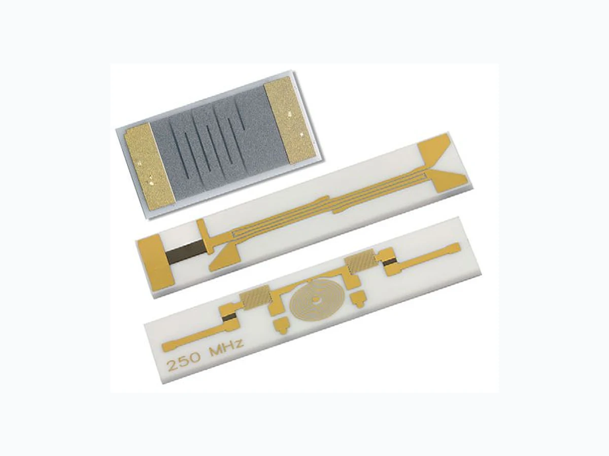
Vishay EFI conductor resistor patterned subs trates with optional overcoat coatings ar e used in the hybrid circuit, microwave, and telecommunications industries. These co nductor resistor patterns are precisely manufactured to be used for precision current flow, voltage division and RF / Microwave designs. Resistor overcoat options are used for resistor protection and can be applied and patterned to match the cond uctor and / or resistor pattern. The cond uctor resistor patterned substrates are manufactured using Vishay Electro-Films (EFI) sophisticated thin film equipment and manufacturing technology. The custom specialty film substrates are visually inspected to MIL-STD-883, method 2032 class H or K. THIN FILM DESIGN GUIDELINES For further detail, please reference document: Thin Film Design Guide for RF and UWave Substrates (www.vishay.com/doc?49109). SUBSTRATE MATERIALS For substrate materials and their properties, please reference datasheet: SPF1 (www.vishay.com/doc?61105). METAL SYSTEM AND CONDUCTOR PATTERNING For metal system options and metal patterning guidelines, please reference datasheet: SPF2 (www.vishay.com/doc?61110). INTEGRATING THIN FILM RESISTORS Vishay EFI offers two thin film resistor film choices of lithographically patterned Tantalum Nitride (TaN) or Nickel Chromium (NiCr). The resistive film should be sele cted based upon application-specific requ irements such as performance, assembly packaging needs, and temperature exposu re. The table below summarizes the key standard parameters of these resistor materials. Notes (1) 1000 h at 125 ºC in air (2) Special tolerances available STANDARD THIN FILM RESISTOR PARAMETERS MATERIAL TCR (ppm/°C) STANDARD SHEET RESISTIVITY 99.6 % Al2O3 (/sq) STANDARD SHEET RESISTIVITY AIN, BeO (/sq) STABILITY (1) TOLERANCE (2) TaN ± 50 20 to 125 25 to 100 < 0.1 % 0.1 % to 20 % NiCr ± 25 25 to 225 50 to 150 < 0.1 % 0.1 % to 20 %
www.vishay.com Vishay Electro-Films Revision: 26-Sep-2018 2 Document Number: 61111 For technical questions, contact: efi@vishay.com THIS DOCUMENT IS SUBJECT TO CHANGE WITHOUT NOTICE. THE PRODUCTS DESCRIBED HEREIN AND THIS DOCUMENT ARE SUBJECT TO SPECIFIC DISCLAIMERS, SET FORTH AT www.vishay.com/doc?91000 CURRENT DENSITY To ensure optimal Resistor performance, the design engineer must consider the self-h eating effects of the operating resistor and understand the power dissipation characteristics of the environment. A complete thermal analysis should be performed by the design engineer to ensure proper thin film resistor design. The following table lists curre nt density standards for common materials. RESISTOR DESIGN After the thin film resistor va lues have been determined and a metallization film selected per SPF1 and SPF2 datasheets, the thin film resistor layout can be designed. There are two typical approaches for accomplishing this: the block-style resistor (see Fig. 1) or serpentine- style resistor (see Fig. 2). With both design approaches, it is standard to employ a laser trim process to trim the resistor to the desired value an d tolerance. Vishay EFI empl oys both scrub (edge) trim ming and plunge trimming techniques to achieve the desired resistor value. Fig. 1 - Probe pad and artwork overlap requirements (minimum) Fig. 2 - Serpentine resistor with two areas for laser trim All high frequency resistors should be Edge trimmed to value to preserve frequency response. VEFI can also supply resistors of 20 % tolerance (10 % special) or looser tolerances which are designed to 100 % of bake to value with no laser trimming. CURRENT DENSITY SHEET RESISTANCE Al2O3 SILICON QUARTZ AIN BeO 25 /sq 4 mA/mil 20 mA/mil 0.5 mA/mil 19 mA/mil 32 mA/mil 50 /sq 2 mA/mil 10 mA/mil 0.25 mA/mil 9.5 mA/mil 16 mA/mil 100 /sq 1 mA/mil 5 mA/mil 0.125 mA/mil 4.7 mA/mil 8 mA/mil 200 /sq 0.5 mA/mil 2.5 mA/mil 0.062 mA/mil 2.3 mA/mil 4 mA/mil Resistor length 0.002" (50.8 μm) Artwork overlap 0.002" (50.8 μm) 0.0005" (12.7 μm) 0.003" (76.2 μm) Probe pad Laser trim example Laser kerf= 0.0015" (38.1μm) Resistor squares compensated for laser kerf Serpentine areaLink area RESISTOR DESIGN RULES PARAMETER VALUES COMMENTS Min. resistor dimension 0. 002" x 0.002" (50 μm x 50 μm) Min. probe pad dimension 0. 003" x 0.003" (75 μm x 127 μm) For resistors < 1000 , use probe pad size of 0.006" (152 μm) x 0.008" (203 μm) Min. conductor/resistor design overlap 0.0 02" (50 μm) See Fig. 1 Resistor layout dimensions (block resistor/serpentine resistor) 100 % of nominal value / 100 % of nominal resistor value plus laser kerfs of 0.5 mil 2/sq Resistor trim Scrub, plunge, or bake to value Bake to value ± 10 % or 20 %
www.vishay.com Vishay Electro-Films Revision: 26-Sep-2018 3 Document Number: 61111 For technical questions, contact: efi@vishay.com THIS DOCUMENT IS SUBJECT TO CHANGE WITHOUT NOTICE. THE PRODUCTS DESCRIBED HEREIN AND THIS DOCUMENT ARE SUBJECT TO SPECIFIC DISCLAIMERS, SET FORTH AT www.vishay.com/doc?91000 PROTECTIVE COATING Vishay Electro-Films (EFI) has developed several patternable overcoat options to protect the resistors and other critical areas from mechanical damage during handling. It is essential to overcoat resistors of 0.1 % or tighter tolerances to maintain tolerance during assembly and test of the hybrid, and it is beneficial to overcoat all resistors. Notes (1) Special tolerance of ± 0.001" available (2) Minimum gap in polyimide pattern is 0.0015" x 0.003" In summary NiCr will perform at higher sheet resistance with lower TCR than TaN giving higher resistance values in less area. TaN will continue to perform in a moisture environment but NiCr will require a hermetic package to maintain resistance values. Both resistive films will work in highly demanding environments for a wide range of applications with VEFI thin film technology. PROTECTIVE COATING APPLICATIONS OVERCOAT TYPICAL THICKNESS (Å) APPLICATIONS Silicone nitride 4000 to 6000 Resistor overcoat with fine trim capability and integrated capacitor Polyimide 50 000 to 80 000 Resistor overcoat and solder dam PROTECTIVE COATING GUIDELINES OVERCOAT TYPICAL THICKNESS (Å) MIN. FEATURE SIZE MIN. METAL OVERLAP PATTERN TOLERANCE (1) Silicone nitride 4000 to 6000 0.004" x 0.004" 0.002" ± 0.002" Polyimide 50 000 to 80 000 0.004" x 0.004" (2) 0.001" ± 0.002" GLOBAL PART NUMBER INFORMATION Custom Global Part Number: PSS205687-00N Custom Global Part Number Description: Specialty Films Custom 205687-00N PSS205687 - 00 N MODEL CUSTOM PART NUMBER INTERNAL REVISION VARIANT A = AlN B = BeO F = ferrite/ garnet K = zirconia N = resistor conductor CONTACT INFORMATION For design assistance, contact: efi@vishay.com
www.vishay.com Vishay Revision: 01-Jan-2022 1 Document Number: 91000 Disclaimer ALL PRODUCT, PRODUCT SPECIFICATIONS AND DATA AR E SUBJECT TO CHANGE WITH OUT NOTICE TO IMPROVE RELIABILITY, FUNCTION OR DESIGN OR OTHERWISE. Vishay Intertechnology, Inc., its affiliates, agents, and employee s, and all persons acting on it s or their behalf (collectivel y, “Vishay”), disclaim any and all liability for any errors, inaccuracies or incompleteness contained in any datasheet or in any other disclosure relating to any product. Vishay makes no warranty, representation or guarantee regarding the suitability of the products for any particular purpose or the continuing production of any product. To the maximum extent permitted by applicable law, Vishay disclaims (i) any and all liability arising out of the application or use of any product , (ii) any and all liability, including without limitation specia l, consequential or incidental damages, and (iii) any and all implied warranties, incl uding warranties of fitness for particular purpose, non-infringement and merchantability. Statements regarding the suitability of pro ducts for certain types of applications are based on Vishay's knowledge of typical requirements that are often placed on Vishay products in ge neric applications. Such statements are not binding statements about the suitability of products for a particular application. It is the customer's responsibility to validate that a particular product with the properties described in the product specification is suitable for use in a particular application. Parameters provided in datasheets and / or specificat ions may vary in different applications and performance may vary over time. All operating parameters, including typical parameters, must be validated for each customer application by the customer's technical experts. Product specifications do not expand or otherwise modify Vishay's terms and conditions of purchase, including but not limited to the warranty expressed therein. Hyperlinks included in this datasheet may direct users to third-party websites. These links are provided as a convenience and for informational purposes only. Inclusion of these hyperlinks does not constitute an endorsement or an approval by Vishay of any of the products, services or opinions of the corporation, organization or individual associated with the third-party website. Vishay disclaims any and all liability and bears no responsibility for the accuracy, legality or content of the third-party web site or for that of subsequent links. Except as expressly indicated in writing, Vishay products are not designed for use in medical, life-saving, or life-sustaining applications or for any other application in which the failure of the Vishay product could result in personal injury or death. Customers using or selling Vishay products not expressly indicated for use in such applications do so at their own risk. Please contact authorized Vishay personnel to obtain written terms and conditions regarding products designed for such applications. No license, express or implied, by estoppel or otherwise, to any intellectual property rights is granted by this document or by any conduct of Vishay. Product names and markings noted herein may be trademarks of their respective owners. © 2022 VISHAY INTERTECHNOLOGY, INC. ALL RIGHTS RESERVED