

 Download PDF
PRF-1150 IXYS
Document overview
- PDF pages: 20
Technical content
Page 1
D I R E C T E D E N E R G Y , I N C . T E C H N I C A L N O T E
PRF-1150 1KW 13.56 MHz CLASS E
RF GENERATOR EVALUATION MODULE
Matthew W. Vania Directed Energy, Inc.
Abstract The PRF-1150 module is a self-contained 1KW 13.56MHz RF source. The module facilitates operation and evaluation of the DEIC420 RF MOSFET gate driver IC and DE275X2-102N06A RF MOSFET in a practical 13.56 MHz RF generator application. It is all-inclusive, pre-tested, and ready to operate.
Directed Energy, Inc.
An IXYS Company
2401 Research Blvd. Suite 108 Fort Collins, CO USA 80526
TEL (970) 493-1901 FAX (970) 493-1903
EMAIL: deiinfo@directedenergy.com http://www.directedenergy.com
Page 2
INTRODUCTION
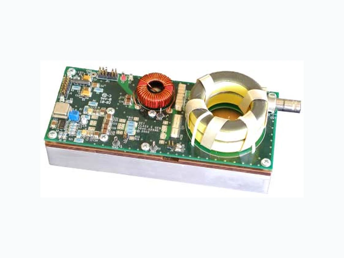
DEI has developed an RF module to demonstrate the capabilities of our DEIC420 RF MOSFET gate driver IC and DE275-102N06X2A 1000V 6A RF MOSFET at ISM frequencies. The PRF-1150 module produces 1000W CW of RF output at 13.56MHz. with 85% DC to RF conversion efficiency. The module is a self-contained RF generator. To produce 1kW of RF output, only external DC power need be applied. The module dimensions as shown in Figure 1 are 6.75” x 3.1” x 2.7” including an air-cooled heatsink and copper heat-spreader. Impingement flow from a standard 4.5” bench fan provides adequate cooling for the 1kW output level. Standard 0.1” dual and single row headers are used for DC input to the module and a single right-angle BNC connector is used for
RF output to a 1kW 50Ω RF load or attenuator.
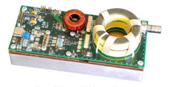
Figure 1: PRF-1150 1KW RF Generator Module
MODULE DESCRIPTION
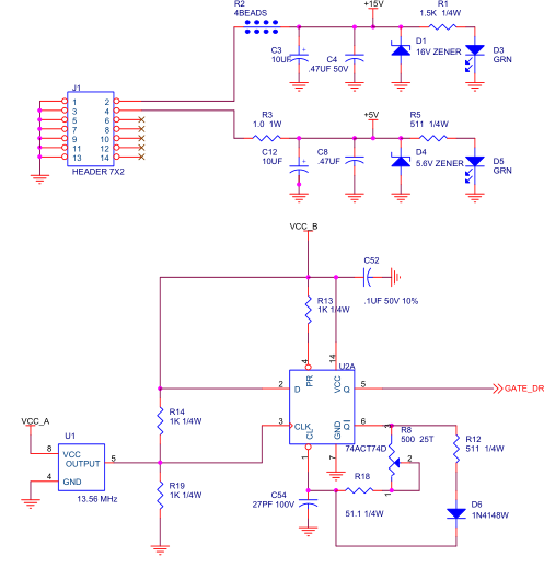
Please refer to Figures 1-6 during this module description. Low-Voltage DC is applied to the module via connector J1. 5V @ 30 ma and 15V @ 3A are applied to J1 pins 4 and 2 respectively. LEDs D3 and D5 glow green if the appropriate voltages are applied. U1 is a 13.56MHz clock providing a 50% DC, 0-5V square wave. U2A provides a pulsewidth adjustable source to drive U4, the DEIC420 gate driver IC.
Page 3
GATE_DRIVE_PULSE
Figure 2: PRF-1150 DC and Gate-Drive Schematic
U4 converts the Gate_Drive_Pulse to a high-current 15Vp waveform capable of driving the gates of U3, the dual 102N06A (DE275X2-102N06A) MOSFET. R10, 11, 15, 16,
and R27-30 are eight, 2Ω resistors in parallel used to dampen the gate drive signal. J3
provides a convenient point to monitor the MOSFET gate signal directly with an oscilloscope. The variable 0-300V VDD supply is connected to JP1. As a safety
measure, LED D2 will glow RED when high-voltage is applied to JP1. L1 is a 21 uH Radio Frequency Choke (RFC) used to block RF from leaving the module via JP1.
Page 4
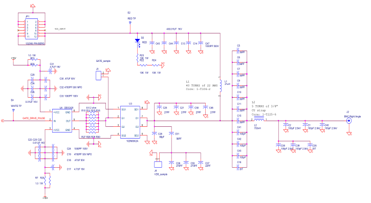
Figure 3: PRF-1150 RF Section Schematic
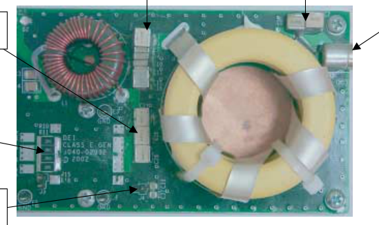
C21, 25, 26, 36, 37, 48, 50, 51 and 53 form the additional shunt C necessary for Class E operation. C36, 37, 51 and 53 form an 11:1 capacitive voltage divider providing a
sample of the drain voltage to J4. C5, 6, 7, 9, 10, 11, 15, 16, 41, 42 and 43 together form the series Tank Capacitor, Ct. L2 functions as both the main Tank inductor and as
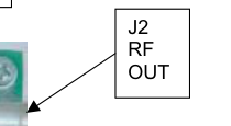
part of the output “L-match” matching the tank impedance to the RF load. C1, 2, 35 and C38-40 form the shunt Co portion of the output L-match network. J2 is a BNC connector for the module RF output signal.
Page 5
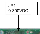
L2
L1
Tank L
RFC
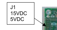
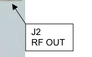
U1 OSC
Figure 4: PRF-1150 Top View
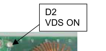
D3 15V OK
D5 5V OK
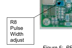
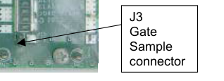
Figure 5: PRF-1150 Left Side Top View
Page 6
Ctank
Load C
(Ct)
(Co)
Drain C (Cd)
8X 2 Ω Gate R
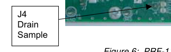
Figure 6: PRF-1150 Right Side Top-View
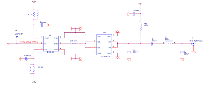
Figure 7: 1KW Class E Functional Diagram
THEORY OF OPERATION
Referring to Figure 7, the active device, U3, is chosen such that it has high-speed turn “on” and “off” characteristics, low RDSon resistance and low COSS and CRSS. As such, it will be an effective low loss switch in its saturated mode of operation. The resonant load network is designed so that its transient response minimizes the power dissipation in the active device during the switching intervals. Figure 8 describes the ideal Class E circuit waveforms. During the “off” state of the active device, the drain current remains at zero while the voltage across the device,
Page 7
Vds, increases to a maximum of 3.5 times Vdd (T0-T1). At the end of the “off” cycle (T1), the voltage across the active device has decreased to zero. At (T1) Vgs is applied and the current through the active device increases toward a maximum of 2.86 times Idc. At the end of the “on” state (T2) the gate drive, Vgs is removed and the current drops to zero before the voltage begins to rise.
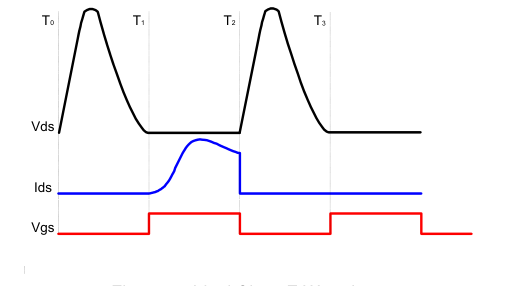
Figure 8: Ideal Class E Waveforms
In principle, there is no appreciable current flowing while drain voltage is present across the device and likewise there is no appreciable voltage (Vds) across the device while drain current is flowing. During switching transitions (T1, T2), both current and voltage have zero crossover values. With switching losses reduced in this manner, the only loss remaining is conduction. The ideal efficiency in a high power Class E amplifier will approach ≥90%. In Figure 7, the resonant load network consists of four passive elements Cd, Ct, Lt, and the effective RF load resistance Rl, connected to BNC connector, J2. The values of these four elements are chosen such that the resonant frequency and Q produce the
ideal waveforms shown in Figure 8. The RF choke (RFC), shown in Figure 7, is essentially high impedance at the operating frequency, fo. Its value is sufficiently high as to act as a constant current source to the resonant circuit
CALCULATING CLASS-E ELEMENT VALUES
Given that the desired RF output power, the frequency of operation and the DC power supply voltage are known and assuming a value for the loaded Q of the resonant load network, we can calculate the values of the Class E resonant elements. The operating frequency in this design is 13.56 MHz. The supply voltage should be chosen for a given output power knowing that the maximum switching device drain voltage can reach 3.56 times VDD. The value of the effective load resistance R is a function of the desired RF output power and the applied DC voltage. The Q of the resonant circuit is dependent on the following factors: 1) the relative importance of the harmonic frequency delivered to
the effective load resistance, and 2) the transient response of the voltage and current waveforms across the active device. If the Q is too low, the voltage across the active
Page 8
device does not discharge to zero prior to the device turning on. Too high of a Q and the voltage across the device discharges too quickly and possibly even swings negative. Please note that Cd, the shunt Capacitance from U3 Drain to Source, is effectively the summation of a physical capacitor and the equivalent Coss of U3. Coss can be estimated from Data Sheet values. A MathCAD model of the Class E topology was used as a guide in the initial design phase of this module. It was intended to use an 8Ω load for the tank load resistance R and keep a low Q of approximately 2 to keep the tank peak voltages below 2KV. The following page is a summary page of those initial design values.
Mathcad Summary Page:
Vdd := 300
106
fo := 13.56 ×
Rl :=
RF load R 50
1.038 103 Po =
×
1.068 103 Vp =
×
Idc = 3.46
Idp = 9.896
Rps = 86.685 − 7
Ltotal =
× 5.597 10 − 10
TankC =
× 7.336 10 − 10
Cdrain =
× 2.239 10
− 10
Cmatchshunt=
× 5.379 10
R :=
tank load R 8.0
Ql :=
tankQ 2.0
Rf output power
Peak drain voltage
Power supply Current
Peak Drain Current
Equivalent PS resistance (ideal)
Tank L
Tank C
Drain shunt C Load shunt C
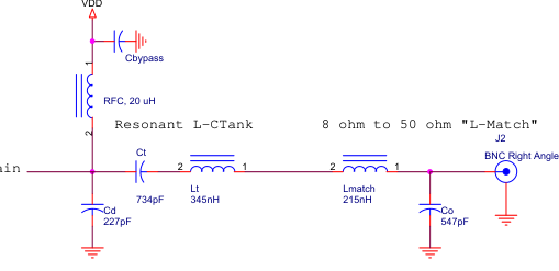
Figure 9 shows impedance match and tank values for the module. The L-match and Co combination match the desired 8Ω load line to BNC connector J2 and the RF load of 50Ω. Lt and Ct form the series-resonant tank. Cd is the shunt drain capacitance required for proper Class E operation. Since the resonant Tank inductor (Lt) is directly in series with the impedance matching inductor (Lmatch), these functionally different inductors are actually implemented as one inductor whose value is the sum of the two.
Page 9
U3 Drain
Figure 9: Simplified Output Tank and L-Match Schematic
These MathCAD results provided a starting point for initial design values. However, It assumes ideal components, includes no parasitics, and assumes an ideal 50% dutycycle (DC) gate drive waveform.
PRACTICAL DESIGN CONSIDERATIONS
The PRF-1150 RF generator was designed using a classical CLASS “E” single-ended switch-mode topology (Figure 7). The module utilizes the DEI DEIC420 RF MOSFET Gate Driver IC driving a DEI DE275X2-102N06A dual MOSFET as the switching device. An L-C tank provides for high-efficiency MOSFET resonant switching action. The addition of additional tank L and a shunt C creates an “L –match” network to transform the tank equivalent R to the 50Ω load. U4, the DEIC420 Gate Driver IC, was chosen for its ability to directly drive the gate of U3. It translates the width adjustable TTL level signal GATE_DRIVE_PULSE to a 15Vp and 8Ap pulse capable of driving U3’s 3600pF gate. Although the VGS threshold is in
the 2.5 to 5V range, to ensure device saturation and ensure minimal I2 \* RDSon losses, the gate is driven to 15Vp. Driving a MOSFET gate in Class E operation with sub-10ns rise and fall times can require a large amount of power. The calculated drive power requirement for the DE275X2-102N06A with 3600pF, and 15Vp gate voltage swing is 11W using P= Ciss\*V2\*f. In addition, the DEIC420 has internal timing and anti-cross-conduct circuitry that dissipate additional power. The total drive power is on the order of 45W (15V@3A). When the DEIC420 is used as a high current driver, several design and layout parameters are critical for best results. Physically locating the driver and MOSFET
close to one another in the PCB layout is important. It is critical to minimize stray inductance between the driver output terminal and the MOSFET gate terminal, as ringing of the drive signal may result. In this design an 0.25Ω resistor was installed to dampen a gate drive ring. As peak currents can approach 20A, VCC bypassing, layout symmetry, and device grounding are critical. VCC bypassing capacitors should be located as closely as possible to the DEIC420 VCC to GND pins. This is critical as the initial instantaneous current on device turn-on is provided from stored energy in the bypass capacitors.
Page 10
These capacitors should be low inductance and low ESR types chosen specifically for pulse applications. SMT caps are recommended for their low inductance package and density. This allows easy parallelling of several caps very close to the DEIC420 while minimizing lead and layout inductance. Figure 3 shows the actual circuit values chosen for this design. Finally, on device “turn-off” the gate must be discharged rapidly, and the ground return path from the MOSFET source to driver return leads must be low inductance and low impedance. This is usually ensured during layout by keeping the driver and MOSFET physically close, and maintaining symmetric return paths including
a ground plane on the PCB. Figure 9 describes a typical gate drive pulse for the PRF- 1150 module. The DE275X2-102N06A MOSFET is a dual device in that it houses two independent MOSFETS in one package. It maintains a low RDSon (2.0Ω/2 = 1Ω), a 12A current rating, and thermal capabilities of 560W Pd @ 25oC and a theta Junction-to-Heatsink of 0.26oC/W. The 1KV part was chosen because the peak drain voltage can approach 3.5 X VDD. The implementation of the Output Tank and matching network given target design values from MathCAD is straightforward. All capacitors are low ESR porcelain ceramic capacitors chosen for their low-loss RF characteristics. Note that the drain peak voltage
can approach 1KV, and due to the resonant tank action the tank L/C common point can approach Ql x Vp, or 2KVp. Appropriate voltage rated parts should be used. Several manufacturers including ATC (American Technical Ceramics), Murata Erie, and Dielectric Labs all supply appropriate capacitors for this application. To minimize localized capacitor heating and to provide adequate design margin, several capacitors are used in parallel. Similarly, the Tank and matching network circulating currents can easily approach 20Ap. Tank inductor L2 was designed for the best minimum-loss design that would fit into the available PCB footprint. The conductor is made from silver-plated 3/8” copper
strap. The silver plating is used to provide the lowest conductive losses in a practical design format and provides a 3% decrease in Rac over standard copper strap material. This directly corresponds to a 3% decrease in conduction loss. Iron powder material for the toroid was chosen for it’s low permeability, good temperature stability, and high Curie temperature.
OPERATIONAL WAVEFORMS
Although careful initial design will minimize module tuning, some deviation from ideal is to be expected. The best approach to fine tuning this topology is to observe the drain waveform with an oscilloscope. There are two sample connectors on this module designed to support module testing. J4 provides an AC coupled 11:1 voltage sample of the MOSFET drain waveform. For 1kW output a quasi-sine of 800/11 = 73Vp will be available for monitoring. This is useful if a 100:1 voltage probe is unavailable or for implementing protection circuitry for the module. Figure 10 represents a good goal for the drain waveform. J3 provides a direct sample of the MOSFET gate drive signal. It is intended that a 50Ω
coax cable be plugged into connector J3. The gate drive can then be directly monitored
Page 11
on an oscilloscope. A 50Ω termination is recommended at the scope input. When correctly operating, you can expect to see the following waveforms:
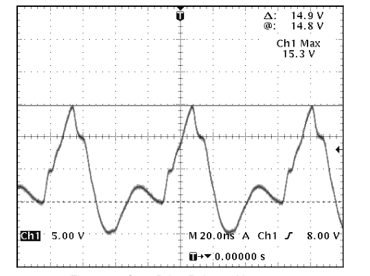
Figure 9: Gate Drive Pulse at U3 gate
Figure 10 shows the Drain of U3 at 1KW output power. This represents a classical tune for best efficiency and minimal switching losses. Note that at both “turn-off” and “turn-on” times the waveform is gently rounded as it approaches the ground reference. This ensures the best efficiency by maintaining the MOSFET at zero volts Vds during the switching intervals. Please note that U.S. patent #5,187,580 describes a specific Class “E” tune condition where the Drain waveform, as it approaches VDSsat on MOSFET turn-on, is NOT smooth and rounded, but contains a straight rear edge or distinct “step” in the VDS waveform at “substantial voltage”. The reader is encouraged to familiarize himself with
the references at the end of this technical note for further information.
Page 12
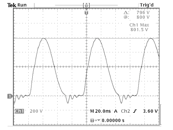
Figure 10: Drain Waveform @ U3, Drain, 1KW output power
The quasi-sine drain waveform of U3 is converted to a sine wave by the resonant action of the tank network (Ct and Lt in Figure 7). The higher the Q of the resonant tank, the more pure the sine wave is and the lesser the harmonic content in the RF output. Figure 11 shows the output waveform at the 50Ω load after the output tank and matching network. Figure 12 is a frequency domain measurement of the PRF-1150 harmonic content. The output power is 1KW (60 dBm) and note the second and all higher harmonics are greater than 30 dB below the fundamental signal (≤ -30dBc). Further filtering can easily be added in the output-matching network if additional harmonic suppression is required.
Page 13
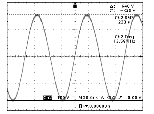
Figure 11: RF output Waveform J2, 1KW output power
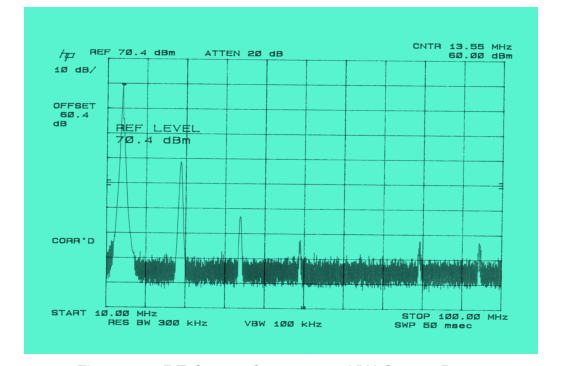
Figure 12: RF Output Spectrum, 1KW Output Power
Page 14
TEST DATA
Typical module data is shown in Table 1. Data are taken in 100W increments and the VDS power supply voltage, drain current (Id), and U3 peak Drain voltages were recorded. The fifth and sixth columns are the calculated efficiency (Po/(VDS\*Id)) and PS load-line (LL=VDS/Id) values, respectively.
| VDS | Id | Po | Vdrain | Efficiency | PS load line |
| V | A | W | Vp | % | Ω |
| 89.7 | 1.40 | 100 | 231 | 79.6 | 64.1 |
| 128.4 | 1.86 | 200 | 334 | 83.7 | 69.0 |
| 157.5 | 2.23 | 300 | 411 | 85.4 | 70.6 |
| 181.7 | 2.56 | 400 | 476 | 86.0 | 71.0 |
| 203.4 | 2.86 | 500 | 534 | 85.9 | 71.1 |
| 222.9 | 3.13 | 600 | 588 | 86.0 | 71.2 |
| 241.1 | 3.39 | 700 | 636 | 85.6 | 71.1 |
| 257.9 | 3.63 | 800 | 683 | 85.5 | 71.0 |
| 273.8 | 3.85 | 900 | 723 | 85.4 | 71.1 |
| 289.1 | 4.07 | 1000 | 763 | 85.0 | 71.0 |
Table 1: PRF-1150 Test Data
Table 2 is a comparison of the expected operating parameters of U3, the DE275- 102N06A MOSFET, and key data sheet parameters. The Pd and Tj calculations assume a 30oC heatsink temperature rise above a 25oC ambient. Note that the peak drain voltage, peak current, junction temperature, and expected power dissipation are all well within the safe operating parameters for this device with at least a 20% operating margin.
| Parameter | Operating (RF) | Device Maximum at 55oC Case Temperature | Margin (%) |
|---|---|---|---|
| VDSmax (Vp) | 800 | 1000 | 20 |
| IDp (Ap) | 9.9 | 48 | 79 |
| Pd (W) | 177 | 445 | 60 |
| Tj (oC) | ≤101 | 175 | ≥42 |
Table 2: U3, DEI DE275X2-102N06A MOSFET Design Margins
SPICE ANALYSIS
The initial MathCAD analysis assumed ideal components, included no parasitics, and assumed an ideal 50% duty-cycle (DC) gate drive waveform. A better basis for future design was desired. As a result, further analysis of the PRF-1150 was performed using
Page 15
SPICE. DEI provides Level 3 SPICE models in ASCII text format on our website (http://www.directedenergy.com/spice.htm). Figure 13 shows the .subckt used in the simulation of the 102N06A MOSFET used in the PRF-1150 module.
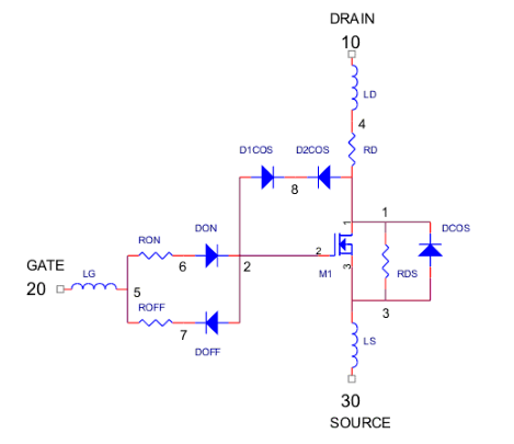
\*SYM=POWMOSN .SUBCKT 102N06A 10 20 30 \* TERMINALS: D G S \* 1000 Volt 6 Amp 2.0 Ohm N-Channel Power MOSFET M1 1 2 3 3 DMOS L=1U W=1U RON 5 6 .5 DON 6 2 D1 ROF 5 7 1.0 DOF 2 7 D1 D1CRS 2 8 D2 D2CRS 1 8 D2 CGS 2 3 1.9N RD 4 1 1.7 DCOS 3 1 D3 RDS 1 3 5.0MEG LS 3 30 .5N LD 10 4 1N LG 20 5 1N .MODEL DMOS NMOS (LEVEL=3 VTO=4 KP=2.3) .MODEL D1 D (IS=.5F CJO=10P BV=100 M=.5 VJ=.2 TT=1N) .MODEL D2 D (IS=.5F CJO=400P BV=1000 M=.6 VJ=.6 TT=1N RS=10M) .MODEL D3 D (IS=.5F CJO=400P BV=1000 M=.35 VJ=.6 TT=400N RS=10M) .ENDS
Figure 13: DE275X2-102N06A SPICE Model
Page 16
ORCAD PSPICE AD version 9.2.1 was used as the simulation platform. Figure 14 describes the circuit schematic and values used in the simulation.
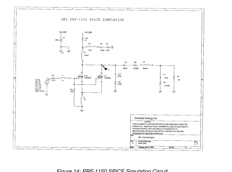
Figure 14: PRF-1150 SPICE Simulation Circuit
Each of the critical circuit waveforms described in the “operational waveforms” section above is also presented here via the SPICE simulation for comparison. Figure 15 shows the MOSFET gate drive signal. Figure 16 describes the drain voltage at 1kW of RF output power. Finally, Figure 17 displays the output sine wave at the RF load. Table 3 directly compares the measured test data from the PRF-1150 bench testing to the SPICE simulation data.
Page 17
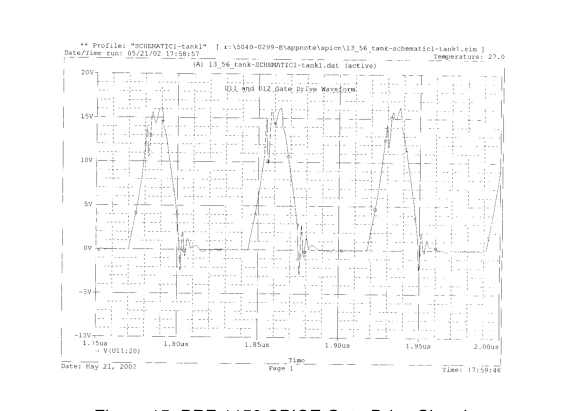
Figure 15: PRF-1150 SPICE Gate Drive Signal
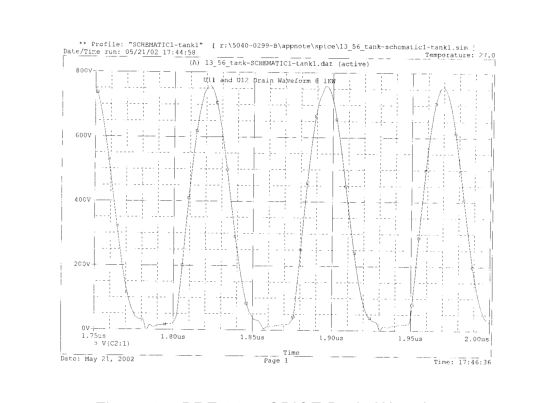
Figure 16: PRF-1150 SPICE Drain Waveform
Page 18
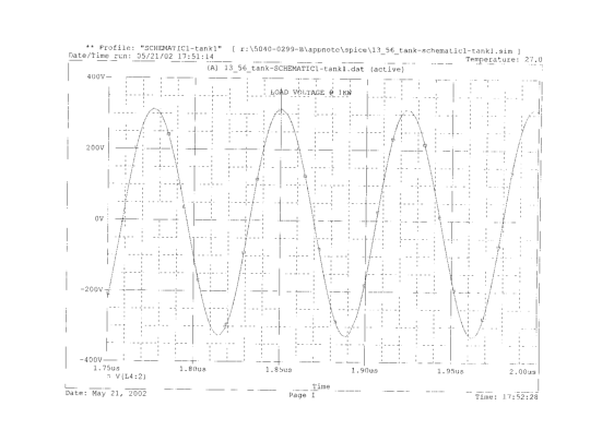
Figure 17: PRF-1150 SPICE RF Output signal @ 1kW and 50Ω
| Parameter | SPICE | Bench Data |
|---|---|---|
| PinDC (W) | 1098 | 1177 |
| PoutRF (W) | 1003 | 1000 |
| Efficiency (%) | 91.4 | 85.0 |
| PS current (Adc) | 3.8 | 4.1 |
| Drain Voltage (Vp) | 759 | 763 |
| PS Voltage @ 1kW (V) | 289 | 289.1 |
Table 3: SPICE and Test Data Comparison
CONCLUSION
The PRF-1150 RF generator module produces 1KW from a single DE275X2-102N06A dual MOSFET device with ≥85% DC to RF conversion efficiency. Based on a traditional Class “E” topology, a 1 kW, high-efficiency, air-cooled module, with a volume of less than 57 cubic inches was successfully designed and built and is available for purchase from DEI. The density of packaging shows what is currently possible using SMT. The DEIC420 gate driver IC functions successfully as a dedicated MOSFET gate driver for the DE275X2-102N06X2A MOSFET device operated with both internal MOSFET devices in parallel. Its 20Ap capability successfully drives ≥3600pF of Ciss at 13.56MHz. Because of the sub-10nS rise-times and high peak currents involved, a
discussion of key layout and design issues is included.
Page 19
Ideal waveforms as well as bench test data are included to help in the understanding of Class E operation, as well as to provide a basis for design of customer-specific modules. The successful implementation of an output L-C Tank Circuit is key to a highefficiency Class E design. This design incorporates a “Low Q” design to intentionally keep peak voltages and resonant circulating currents as low as practically possible. These efforts along with the use of low-ESR porcelain “RF” capacitors, powdered-iron toroids, and an extremely low-loss inductor design keep component heating to a minimum. Even with the low Q design, the 1KW harmonic spectrum of the RF output
shows all harmonics at least ≤ -30dBc. Test data shows ≥85% efficiency over an output power range of 300-1000W of output power. A comparison of MOSFET operating conditions shows ≥20% margin for key operating parameters including VDSmax, ID, Pd, and Tjmax at the 1KW output level. Although several design methods are available, SPICE simulation shows very good correlation between bench test data and simulation results. As a result, we recommend SPICE analysis for designing the Class E topology. DEI provides MOSFET SPICE models that are easily incorporated into standard “off the shelf” SPICE programs and design suites. The PRF-1150 provides the customer with a functional, compact, and tested RF
module. It can be used stand-alone in RF generator applications, as the basis of new design insight, or improved upon to meet customer needs. It is an ideal building block for high-density low and medium power plasma etching and deposition applications. Complete PRF-1150 modules are available pre-tested both with and without heatsinks from DEI. Please email deiinfo@directedenergy.com for more information.
Page 20
REFERENCES
Further information on the Class E topology and its design is available in the following references. US Patent #3,919,656 HIGH-EFFICIENCY TUNED SWITCHING POWER AMPLIFIER Nathan O. Sokal; Alan D. Sokal November 11, 1975 US Patent #4,607,323 CLASS E HIGH-FREQUENCY HIGH-EFFICIENCY DC/DC POWER CONVERTER Nathan O. Sokal; Richard Redl August 19, 1986 US Patent #5,187,580 HIGH POWER SWITCH-MODE RADIO FREQUENCYAMPLIFIER METHOD AND APPARATUS Robert M. Porter; Michael L. Mueller February 16, 1993 Herbert L. Krauss and Charles W. Bostian Solid State Radio Engineering Copyright 1980, John Wiley & Sons ISBN 0-471-03018-X pp 448-454 Mihai Albulet
RF POWER AMPLIFIERS
Copyrighted 2001, Noble Publishing ISBN 1-884932-12-6 pp 215-301
Directed Energy, Inc.
An IXYS Company
2401 Research Blvd. Suite 108 Fort Collins, CO USA 80526
TEL (970) 493-1901 FAX (970) 493-1903
EMAIL: deiinfo@directedenergy.com http://www.directedenergy.com