
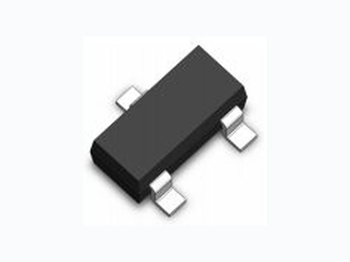
PMV27UPEA LEIDITECH
Document overview
- Manufacturer or author: Provided By www.digicamel.com(FREE DATASHEET DOWNLOAD SITE)
- PDF pages: 5
Technical content
-20V P-Channel Enhancement Mode MOSFET
Description
D G S Package Marking and Ordering Information Device Marking Device Device Package Reel Size Tape width Quantity A5SHB SOT-23 Ø180mm 8 mm 3000 units Dimensions SOT-23 Pin Configuration Rev : 01.07.2021 1/ www.leiditech.com Absolute Maximum Ratings (TC=25℃unless otherwise noted) to provide excellent RDS(ON), low gate charge and operation with gate voltages as low as 4.5V. This device is suitable for use as a Battery protection or in other Switching application. VDS = -20V ID =-4.9A RDS(ON) < 38mΩ @ VGS=-4.5V Battery protection Load switch Uninterruptible power supply Symbol Parameter Rating Units V DS Drain Source Voltage V V GS Gate Sou r ce Voltage V I D A =25 Continuous Drain Current, V GS 4.5V 4.9 A I D A =70 Continuous Drain Current, V GS 4.5V 3.9 A I DM Pulsed Drain Current A P D A =25 Total Power Dissipation 1.31 W P D A =70 Total Power Dissipation 0.84 W T STG Storage Temperature Range 55 to 150 T J Operating Junction Temperature Range 55 to 150 R θ JA Thermal Resistance Junction Ambient 120 R θ JA Thermal Resistance Junction Ambient 10s) PMV27UPEA The uses advanced trench technology PMV27UPEA PMV27UPEA
Rev : www.leiditech.com Electrical Characteristics (TJ=25℃, unless otherwise noted) S ymbol Parameter Conditions Min. Typ. Max. Unit BV DSS Drain Source Breakdown Voltage V GS =0V , I D 250uA --- --- V BV DSS T J BV DSS Temperature Coefficient Reference to 25 , I D 1mA --- 0.014 --- R DS(ON) Static Drain Source On Resistance V GS 4.5V , I D 4.9A --- m Ω V GS 2.5V , I D 3.4A --- V GS 1.8V , I D --- V GS(th) Gate Threshold Voltage V GS DS , I D 250uA 0.4 --- 1.0 V V GS(th) V GS(th) Temperature Coefficient --- 3.95 --- mV/ I DSS Drain Source Leakage Current V DS 16V , V GS =0V , T J =25 --- --- uA V DS 16V , V GS =0V , T J =55 --- --- I GSS Gate Source Leakage Current V GS 12V , V DS =0V --- --- 100 nA gfs Forward Transconductance V DS 5V , I D --- 12.8 --- S Qg Total Gate Charge ( 4.5V) VDS=-15V , VGS=-4.5V , ID=-3A --- 10.2 14.3 nC Qgs Gate Source Charge --- 1.89 2.6 Qgd Gate Drain Charge --- 3.1 4.3 Td(on) Turn On Delay Time VDD=-10V , VGS=-4.5V , RG=3.3 , ID=-3A --- 5.6 11.2 ns Tr Rise Time --- 40.8 Td(off) Turn Off Delay Time --- 33.6 Tf Fall Time --- Ciss Input Capacitance V DS 15V , V GS =0V , f=1MHz --- 857 1200 pF Coss Output Capacitance --- 114 160 C rss Reverse Transfer Capacitance --- 108 151 I S Continuous Source Current 1,4 V G D =0V , Force Current --- --- 4.9 A I SM Pulsed Source Current 2,4 --- --- A V SD Diode Forward Voltage V GS =0V , I S 1A , T J =25 --- --- V t rr Reverse Recovery Time I F 3A , di/dt=100A/µs , T J =25 --- 21.8 --- nS Q rr Reverse Recovery Charge --- 6.9 --- nC Note : 1 .The data tested by surface mounted on a 1 inch2 FR-4 board with 2OZ copper. 2.The data tested by pulsed , pulse width △ 300us , duty cycle △ 2% 3.The power dissipation is limited by 150℃ junction temperature 4.The data is theoretically the same as ID and IDM , in real applications , should be limited by total power dissipation. 01.07.2021 PMV27UPEA
Rev : www.leiditech.com 3/5 Typical Characteristics Fig. Normalized R DSON vs. T J 01.07.2021 PMV27UPEA
Rev : www.leiditech.com 4/5 Fig. Normalized Maximum T ransient Thermal Impedance Fig. Switching Time Waveform Fig. Gate Charge Waveform 01.07.2021 PMV27UPEA
Shanghai Leiditech Electronic Co.,Ltd Email: sale1@leiditech.com Tel : +86- 021 50828806 Fax : +86- 021 50477059 Rev : www.leiditech.com Package Mechanical Data-SOT-23 Symbol Dimensions in Millimeters MIN. MAX. A 0.900 1.150 A1 0.000 0.100 A2 0.900 1.050 b 0.300 0.500 c 0.080 0.150 D 2.800 3.000 E 1.200 1.400 2.250 2.550 e 0.950TYP 1.800 2.000 L 0.550REF 0.300 0.500 θ 01.07.2021 PMV27UPEA