
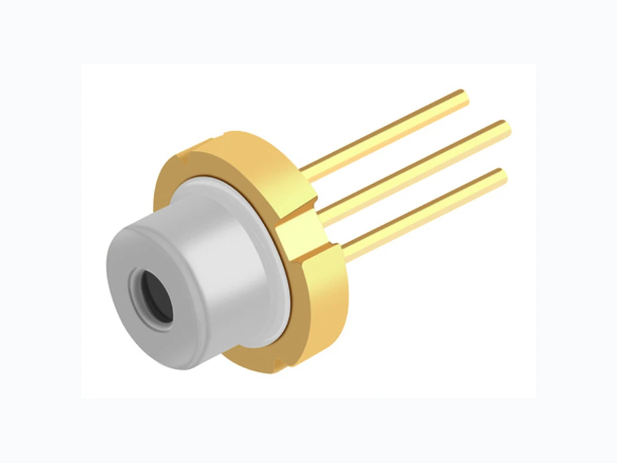
PLT5520 OSRAM
Document overview
- Manufacturer or author: Provided By www.digicamel.com(FREE DATASHEET DOWNLOAD SITE)
- PDF pages: 10
Technical content
Features
- Optical output power (continuous wave): 30 / 50 mW (Tcase = 25 °C)
- Typical emission wavelength: 520 nm
- Efficient radiation source for cw and pulsed operation
- Single transverse mode semiconductor laser
- High modulation bandwidth
- TO56 package with photo diode
Applications
- Laser projection
- Laser shows
- Biomedical Applications
- Metrology Safety Advice Depending on the mode of operation, these devices emit highly concentrated visible light which can be hazardous to the human eye. Products which incorporate these devices have to follow the safety precautions found in IEC 60825-1 “Safety of laser products”.
23.05.2017 2 DRAFT - This design is for Reference only. Subject to change – may be necessary in a limited number of cases. Version 0.3 PLT5 520
Ordering Information
Operation outside these conditions may damage the device. Operation at maximum ratings may influence lifetime. Type: Optical Output Power Ordering Code Popt (Tcase = 25°C) PLT5 520_B1-3 50 mW Q65111A5771 PLT5 520_B1-6 30 mW Q65111A6145 Parameter Symbol Values Unit min. max. Operating Current IF 200 mA Operating Temperature Tcase - 20 + 60 °C Storage Temperature Tstg - 40 + 85 °C Reverse Voltage VR 2V Soldering Temperature max. 10 sec. Tsolder 260 °C Junction temperature Tj 150 °C
Version 0.3 PLT5 520 23.05.2017 3 DRAFT - This design is for Reference only. Subject to change – may be necessary in a limited number of cases. Laser Characteristics (Tcase = 25 °C) Parameter Symbol Values Unit min. typ. max. Emission Wavelength1) 2) 3) 1) Standard operating conditions refer to a continuous wave output power of Popt = 50 mW (B1-B3) and Popt = 30 mW (B4-B6). 2) Popt, λpeak, and VF is measured with an internal re producibility of ±7%, ±0.3 nm, and ±0.05 V, respectively (acc. to GUM with a coverage factor of k = 3). 3) Monitor current refers to a reverse voltage of V = 5 V. B1; B4 B2; B5 B3; B6 λpeak 510 515 520 515 520 530 nm nm nm Spectral Width (FWHM) 1) Δλ –2– n m Threshold Current B1-B3 B4-B6 Ith – mA mA Operating Current 1) 2) B1-B3 B4-B6 IF – 125 100 160 140 mA mA Operating Voltage 1) 2) B1-B3 B4-B6 VF – 6.9 6.5 8.0 8.0 V V Beam Divergence (FWHM) 1) θ∥ x 5 x 7 x 9 x deg Polarization 1) Pgr – 100:1 – Modulation Frequency f – >100 – MHz Thermal resistance (junction to case) Rth –3 4– K / W Monitor current 1) 3) Im –9 0– µ A
23.05.2017 4 DRAFT - This design is for Reference only. Subject to change – may be necessary in a limited number of cases. Version 0.3 PLT5 520 Optical Output Power (B1-B3) Popt = ƒ (IF) Optical Output Power (B4-B6) Popt = ƒ (IF) Operating Voltage (B1-B3) VF = ƒ (IF) Operating Voltage (B4-B6) VF = ƒ (IF) 0 50 100 150 200 Popt [mW] IF [mA] Tcase=0° C Tcase=4 0° C Tcase=6 0° C Tcase=2 0° C 0 50 100 150 Popt [mW] IF [mA] Tcase=0° C Tcase=4 0° C Tcase=6 0° C Tcase=2 0° C 0 50 100 150 200 0.0 2.0 4.0 6.0 8.0 VF [V] IF [mA] Tcase=0° C Tcase=6 0° C Tcase=4 0° C Tcase=2 0° C 0 50 100 150 200 0.0 2.0 4.0 6.0 8.0 Tcase=0° C Tcase=6 0° C Tcase=4 0° C VF [V] IF [mA] Tcase=2 0° C
Version 0.3 PLT5 520 23.05.2017 5 DRAFT - This design is for Reference only. Subject to change – may be necessary in a limited number of cases. Threshold Current Ith = ƒ (Tcase) Maximum Recommended Operating Current IF = ƒ (Tcase) Spectra (B2; B5) Popt = ƒ (λ) Beam Divergence Popt = ƒ (θ), Tcase = 25 °C 0 2 04 06 0 B4-B6 B1-B3 Ith [mA] Tcase [°C] -20 0 20 40 60 100 120 140 160 180 200 B4-B6 B1-B3 IF [mA] Tcase [mA] 514 516 518 520 522 0.0 0.2 0.4 0.6 0.8 1.0 Popt [a. u.] /s61548 [nm] Tcase=2 0° C Tcase=6 0° C Tcase=4 0° C -40 -20 0 20 40 0.0 0.2 0.4 0.6 0.8 1.0 Popt [a. u.] /s61553 [deg] /s61553 || /s61553 ⊥
23.05.2017 6 DRAFT - This design is for Reference only. Subject to change – may be necessary in a limited number of cases. Version 0.3 PLT5 520 Package Outline Dimensions in mm Pin Connection PD LD
3 Pin 1: LD Cathode
Pin 2: LD Anode, PD Cathode (case) Pin 3: PD Anode
Version 0.3 PLT5 520 23.05.2017 7 DRAFT - This design is for Reference only. Subject to change – may be necessary in a limited number of cases. Tray Dimensions in mm [inches]
23.05.2017 8 DRAFT - This design is for Reference only. Subject to change – may be necessary in a limited number of cases. Version 0.3 PLT5 520 Dimensions of transportation box in mm Barcode-Product-Label (BPL) Transportation Packing and Materials Width Length Height 170 ± 5 265 ± 5 45 ± 5 OHA04563 (G) GROUP: 1234567890(1T) LOT NO: (9D) D/C: 1234 (X) PROD NO: 123456789 (6P) BATCH NO: 1234567890 LX XXXX RoHS Compliant BIN1: XX-XX-X-XXX-X ML X Temp ST XXX °C X Pack: RXX DEMY XXX X_X123_1234.1234 X 9999(Q)QTY: Semiconductors OSRAM Opto XX-XX-X-X LE X XPLELL XX 1234.1234 X X-X-XLLLLLLPL XXXXXX _123_123 -XX--XX- MPLRXX XX X_X123_1 XX-XX MPLPack: RXPack: RX DEMY DEMY MP34MPAMPMMMAMMAMM 9D) D/C:9D) D/C: 12341234MMMMM234 PL Pack: R DEMY AMMMAMAM ) D/C MPMMM C: 123 AMAMAAM (9D) XAAAXAAXAXXAXEXAEXEXEXXXXAXXEXEXX 6789067890EXXXXXXEXEXAEEEXEXEEXXEEXEEXEXEXO: 1234567 ors EEEEEEEEE NO: NO: 1234512345EX ctorsctors ptopto XAX 7890 4 X RXX DEMY X123 9D) D/C: 1234(9
67890 NO: 12345
3_123 -XX- Pack: R DEMY ctors OHA02886 PACKVAR:R077Additional TEXT P-1+Q-1Multi TOPLED Muster OSRAM OptoSemiconductors (6P) BATCH NO: (X) PROD NO: (9D) D/C: 11(1T) LOT NO: 210021998 123GH1234 0 245 (Q)QTY: 2000 0144 (G) GROUP:
260 C RT240 C R
220 C RML
Bin3:Bin2: Q-1-20Bin1: P-1-20 LSY T676 2 2a Temp ST R18 DEMY Barcode label Original packing label Box
Version 0.3 PLT5 520 23.05.2017 9 DRAFT - This design is for Reference only. Subject to change – may be necessary in a limited number of cases. Disclaimer OSRAM OS assumes no liability whatsoever for any use of this document or its content by recipient including, but not limited to, for any design in activities based on this preliminary draft version. OSRAM OS may e. g. decide at its sole discretion to stop developing and/or finalizing the underlying design at any time. Attention please! The information describes the type of component and shall not be considered as assured characteristics. Terms of delivery and rights to change design reserv ed. Due to technical requirements components may contain dangerous substances. For information on the types in question please contact our Sales Organization. If printed or downloaded, please find the latest version in the Internet. Packing Please use the recycling operators known to you. We can also help you – get in touch with your nearest sales office. By agreement we will take packing materi al back, if it is sorted. You must be ar the costs of transport. For packing material that is returned to us unsorted or which we are not obliged to accept, we shall have to invoice you for any costs incurred. Components used in life-support devices or systems must be expressly authorized for such purpose! Critical components* may only be used in life-suppo rt devices** or systems with the express written approval of OSRAM OS. *) A critical component is a componen t used in a life-su pport device or system whose failure can reasonably be expected to cause the failure of that life-support device or system, or to affect its safety or the effectiveness of that device or system. **) Life support devices or systems are intended (a) to be implanted in the human body , or (b) to support and/or maintain and sustain human life. If they fa il, it is reasonable to assume that the health and the life of the user may be endangered. Important notes of operation for laser diode a) Electrical operation OSRAMs laser diodes are designed for maximum performance and reliability. Operating the laser diode above the maximum rating even for very short periods of time can damage the laser diode or reduce its lifetime. The laser diode must be operated with a suitable power supply with minimized electrical noise. The laser diode is very sensitive to electrostatic discharge (ESD). Proper precautions must be taken. b) Mounting instructions In order to maintain the lifetime of the laser diode proper heat management is essential. Due to the design of the laser diode heat is dissipated only through the base plate of the diode‘s body. A proper heat conducting interconnection between the diodes base plate and the heat sink must be maintained.
Version 0.3 PLT5 520 23.05.2017 10 DRAFT - This design is for Reference only. Subject to change – may be necessary in a limited number of cases. Published by OSRAM Opto Semiconductors GmbH Leibnizstraße 4, D-93055 Regensburg www.osram-os.com © All Rights Reserved. Eu RoHS compliant product