

 Download PDF
DATASHEET SEARCH SITE
Document overview
- Manufacturer or author: Provided By www.digicamel.com(FREE DATASHEET DOWNLOAD SITE)
- PDF pages: 22
Technical content
Datasheet sections
- 48 Volt PI31xx
Features
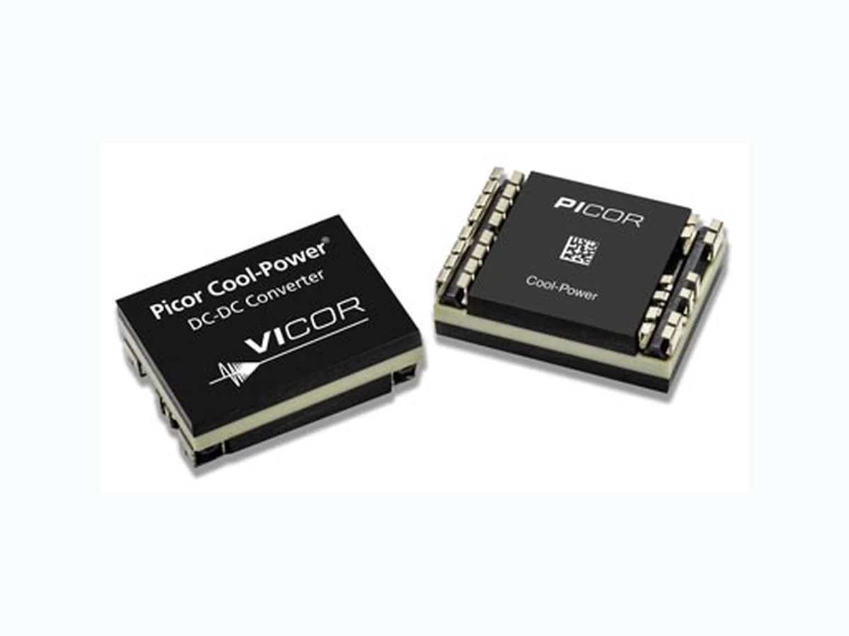
Efficiency up to 89% High switching frequency minimizes input filter requirements and reduces output capacitance Proprietary “Double-Clamped” ZVS Buck-Boost Topology Proprietary isolated magnetic feedback Small footprint (0.57 in2) enables PCB area savings Very low profile (0.265 in) On/Off Control, positive logic Wide trim range +10/-20% Temperature Monitor (TM) & Over-Temperature Protection (OTP) Input UVLO & OVLO and output OVP Over current protection with auto restart Adjustable soft-start 2250 Vdc input to output isolation Surface Mountable 0.87” x 0.65” x 0.265” package
Applications
Space Constrained Systems Isolated Board Level Power Network Power Systems Telecommunications Distributed Power Architecture PoE-Power Over Ethernet IPoL - Isolated Point of Load Power
Package Information
Surface Mountable 0.87” x 0.65” x 0.265” package Weight = 7.8 grams Device Output Voltage IOUT Max Set Range PI3101-00-HVIZ 3.3 V 2.97 to 3.63 V 18 A PI3105-00-HVIZ 12 V 9.6 to 13.2 V 5 A PI3110-01-HVIZ 18 V 16.2 to 19.8 V 3.3 A
Cool-Power® Rev 1.2 vicorpower.com Page 3 of 22 02/2015 800 927.9474
48 Volt PI31xx
TransportCool-Power VIN Vout Iout Max Package Media PI3101-00-HVIZ 36 - 75 V 3.3 V 18 A 0.87” x 0.65” x 0.265” TRAY PI3105-00-HVIZ 36 - 75 V 12 V 5 A 0.87” x 0.65” x 0.265” TRAY PI3110-01-HVIZ 41 - 57 V 18 V 3.3 A 0.87” x 0.65” x 0.265” TRAY Also Available PI3109-01-HVIZ 18 - 36 V 5 V 10 A 0.87” x 0.65” x 0.265” TRAY PI3106-01-HVIZ 18 - 36 V 12 V 4.2 A 0.87” x 0.65” x 0.265” TRAY PI3109-00-HVMZ 16 - 50 V 5 V 10 A 0.87” x 0.65” x 0.265” TRAY PI3106-00-HVMZ 16 - 50 V 12 V 4.2 A 0.87” x 0.65” x 0.265” TRAY PI3111-00-HVMZ 16 - 5 0V 15 V 3.33 A 0.87” x 0.65” x 0.265” TRAY
Cool-Power® Rev 1.2 vicorpower.com Page 4 of 22 02/2015 800 927.9474 +IN to -IN Max Operating Voltage PI3101-00-HVIZ/PI3105-00-HVIZ PI3110-01-HVIZ -1.0 to 75 Vdc (operating) -1.0 to 57 Vdc (operating) +IN to -IN Max Peak Voltage PI3101-00-HVIZ/PI3105-00-HVIZ PI3110-01-HVIZ
100 Vdc (non-operating 100ms) 80 Vdc (non-operating 100ms)
ENABLE to –IN -0.3 to 6.0 Vdc TM to –IN -0.3 to 6.0 Vdc TRIM/SS to –IN -0.3 to 6.0 Vdc +OUT to –OUT See relevant model output section Continuous Output Current See relevant model output section Peak Output Current See relevant model output section Operating Junction Temperature -40 to 125°C Storage Temperature -50 to 125°C Case Temperature During Reflow 245°C Absolute Maximum Ratings
Cool-Power® Rev 1.2 vicorpower.com Page 5 of 22 02/2015 800 927.9474 Functional Block Diagram TRIM/SS +OUT SGND -OUT -IN +IN ENABLE TM LFF RSS CSS INT VREF 1.22V RFB1 CFB1 CFB2 + Error Amp Driver DC Slow Current Limit Driver Synchronous Rectifier DC Output OVP DC Input UVP Input OVP DC DC Fast Current Limit Over Temp DC ENB Period Ramp DC Enable +DC On-Duty Ramp ZVS POWER TRAIN -DC Timing Logic FB FB ENB +5V EA Fault DC 120us delay 120us delay Fault Latch And Reset Logic Reset Fault RUN BIAS START BIAS Vcc Temp Sensor ZVS POWER TRAIN ZVS FB
Cool-Power® Rev 1.2 vicorpower.com Page 6 of 22 02/2015 800 927.9474 +IN Primary side positive input voltage terminals. -IN Primary side negative input voltage terminals. ENABLE Converter enable option, functions as 5V reference and on/off control pin. Pull low for off. TRIM/SS External soft start pin and trim function. Connect to SGND or ENABLE through resistor for trim up or trim down. TM Temperature measurement output pin. SGND Signal ground, primary side referenced. +OUT Isolated secondary DC output voltage positive terminals. -OUT Isolated secondary DC output voltage negative terminals. Pin Description U.S. PATS. LISTED ON PACKING MATERIALS & DATASHEETS MADE IN USA Cool-Power +IN -IN +OUT -OUT SGND TM TRIM/SS ENABLE
Cool-Power® Rev 1.2 vicorpower.com Page 7 of 22 02/2015 800 927.9474 Unless otherwise specified: 36 V < VIN < 75 V, 0 A < IOUT < 18 A, -40°C < TCASE < 100°C(1) [1] These parameters are not production tested but are guaranteed by design, characterization and correlation with statistical process control. Unless otherwise specified, ATE tests are completed at room temperature. [2] Current flow sourced by a pin has a negative sign. Parameter Symbol Conditions Min Typ Max Unit Input Specifications Input Voltage Range V IN 36 48 75 Vdc Input dv/dt (1) V INDVDT VIN = 75 V 1.0 V/µs Input Under-Voltage Turn-on V UVON IO = 1.8 A 32.5 34.0 35.0 Vdc Input Under-Voltage Turn-off V UVOFF IO = 1.8 A 30.5 32.0 33.0 Vdc Input Under-Voltage Hysteresis V UVH IO = 1.8 A 2 Vdc Input Over-Voltage Turn-on V OVON IO = 1.8 A 75.7 78 81.0 Vdc Input Over-Voltage Turn-off V OVOFF IO = 1.8 A 77.7 80.0 82.3 Vdc Input Over-Voltage Hysteresis V OVH IO = 1.8 A 1.6 Vdc Input Quiescent Current I Q VIN = 48 V, ENABLE = 0 V 2.5 mAdc Input Idling Power P IDLE VIN = 48 V, IOUT = 0 A 4 W Input Standby Power P SBY VIN = 48 V, ENABLE = 0 V 0.120 W Input Current Full Load I IN TCASE = 100°C IOUT = 18 A ηFL = 86.5% typical VIN = 48 V 1.43 Adc Input Reflected Ripple Current I INRR LIN = 2 µH CIN = 47 µF 100 V electrolytic 10 mApp+ 2 x 1 µF 100 V X7R ceramic Recommended Ext Input CIN CIN = 47 µF 100 V electrolytic + 2 x 1 µF 100 V X7R ceramic Capacitance C IN = Cbulk + Chf 49 µF Output Specifications Output Voltage Set Point V OUT IOUT = 9 A 3.3 Vdc Total Output Accuracy V OA 0°C <TCASE < 100°C -3 +3 % -40°C <TCASE < 0°C -4 +3 % Output Voltage Trim Range V OADJ -10% 10% % Output Current Range I OUT 18 Adc Over Current Protection I OCP 18.8 26 34 Adc Efficiency – Full Load ηFL TCASE = 100°C, VIN = 48 V 84.5 86.5 % Efficiency – Half Load ηHL TCASE = 100°C, VIN = 48 V 84.5 % Output OVP Set Point V OVP 3.9 4.1 4.3 Vdc Output Ripple Voltage V ORPP COUT = 12 x 10 µF 10 V X7R DC-20 MHz 75 mVpp Switching Frequency f SW 900 kHz Output Turn-on Delay Time t ONDLY VIN = VUVON to ENABLE = 5 V 80 ms Output Turn-off Delay Time t OFFDLY VIN = VUVOFF to ENABLE < 1.8 V 10 µs Soft-Start Ramp Time t SS ENABLE = 5 V to 90% VOUT CREF = 0 230 µs Maximum Load Capacitance C OUT CREF = 1 µF, COUT = Al Electrolytic 10000 µF Load Transient Deviation V ODV IOUT = 25% step 0.1 A/µS COUT = 12 x10 µF 10 V X7R 75 mV IOUT = 25% step 0.1 A/µS Load Transient Recovery Time t OVR COUT = 12 x10 µF 10 V X7R 120 µs VOUT - 1% Maximum Output Power P OUT 60 W Absolute Maximum Output Ratings Name Rating +OUT to -OUT -0.5 V to 4.5 Vdc Continuous Output Current 18 Adc Peak Output Current 34 Adc
Cool-Power® Rev 1.2 vicorpower.com Page 8 of 22 02/2015 800 927.9474 [1] These parameters are not production tested but are guaranteed by design, characterization and correlation with statistical process control. Unless otherwise specified, ATE tests are completed at room temperature. [2] Current flow sourced by a pin has a negative sign. Parameter Symbol Conditions Min Typ Max Unit ENABLE DC Voltage Reference Output V ERO 4.65 4.9 5.15 Vdc Output Current Limit(2) IECL ENABLE = 3.3 V -3.3 -2.6 -1.9 mAdc Start Up Current Limit(2) IESL ENABLE = 1 V -120 -90 -60 µA Module Enable Voltage V EME 1.95 2.5 3.05 Vdc Module Disable Voltage V EMD 1.8 2.35 2.9 Vdc Disable Hysteresis V EDH 150 mV Enable Delay Time t EE 10 µs Disable Delay Time t ED 10 µs Maximum Capacitance C EC 1500 pF Maximum External Toggle Rate f EXT 1H z TRIM/SS Trim Voltage Reference V REF 1.22 Vdc Internal Capacitance C REFI 10 nF External Capacitance C REF 1µ F Internal Resistance R REFI 10 kohms TM (Temperature Monitor) Temperature Coefficient[1] TMTC 10 mV/°K Temperature Full Range Accuracy[1] TMACC -5 5 °K Drive Capability I TM -100 µA TM Output Setting V TM Ambient Temperature = 300°K 3.00 V Thermal Specification Junction Temperature Shutdown[1] TMAX 130 135 140 °C Junction-to-Case Thermal Impedance R ΘJ-C 3 °C/W Case-to-Ambient Thermal Impedance R ΘC-A Mounted on 9 in2 1oz. Cu 6 layer PCB 25°C 8.65 °C/W Regulatory Specification IEC 60950-1:2005 (2nd Edition), EN 60950-1:2006 IEC 61000-4-2 UL 60950-1:2007 CAN/CSA C22.2 NO. 60950-1-07 Recommended Input Fuse Rating I FUSE Fast acting LITTLEFUSE Nano2 Series Fuse 4 10 A
Cool-Power® Rev 1.2 vicorpower.com Page 9 of 22 02/2015 800 927.9474 No Heatsink Thermal Derating Temp °C Load Currrent (Amps)
36 V 0 LFM
48 V 0 LFM
60 V 0 LFM
36 V 200 LFM
48 V 200 LFM
60 V 200 LFM
36 V 600 LFM
48 V 600 LFM
60 V 600 LFM
25 30 35 40 45 50 55 60 65 70 75 80 85 90 95 100 Figure 2 — Load Currrent vs Temperature (without Heat Sink) Figure 1 — Conversion Efficiency Figure 3 — Load Currrent vs Temperature (6.3mm Heat Sink) 11 mm Heatsink Thermal Derating Temp °C Load Currrent (Amps) 25 30 35 40 45 50 55 60 65 70 75 80 85 90 95 100 105 110 Figure 4 — Load Currrent vs Ambient Temperature (11mm Heat Sink) Figure 6 — Start Up C REF = 0 (VIN = 48 V, IOUT = 18 A, CR, COUT = 12 X 10 µF X7R Ceramic) Figure 5 — Start Up C REF = 0 (VIN = 36 V, IOUT = 18 A, CR, COUT = 12 X 10 µF X7R Ceramic) 6.3 mm Heatsink Thermal Derating Temp °C Load Currrent (Amps) 25 30 35 40 45 50 55 60 65 70 75 80 85 90 95 100 105 110 36 V 0 LFM Conversion Efficiency at 100°C Load Curent (Amps) Efficiency 100°C 36 V 1 2 3 4 5 6 7 8 9 10 11 12 13 14 15 16 17 18 100°C 48 V 100°C 60 V
Cool-Power® Rev 1.2 vicorpower.com Page 10 of 22 02/2015 800 927.9474 Figure 8 — Transient Response (V IN = 48 V, IOUT = 9 - 18 A,
0.1 A/µs, COUT = 12 X 10 µF X7R Ceramic)
Figure 7 — Start Up C REF = 0 (VIN = 75 V, IOUT = 18 A, CR, COUT = 12 X 10 µF X7R Ceramic) Figure 9 — Output Ripple (VIN = 48 V, IOUT = 18 A, CR, COUT = 12 X 10 µF X7R Ceramic) Figure 10 — Thermal Image (VIN = 48 V, IOUT = 18 A, CR, 0 LFM Evaluation PCB)
Cool-Power® Rev 1.2 vicorpower.com Page 11 of 22 02/2015 800 927.9474 Unless otherwise specified: 36 V < VIN < 75 V, 0 A < IOUT < 5 A, -40°C < TCASE < 100°C(1) [1] These parameters are not production tested but are guaranteed by design, characterization and correlation with statistical process control. Unless otherwise specified, ATE tests are completed at room temperature. [2] Current flow sourced by a pin has a negative sign. Parameter Symbol Conditions Min Typ Max Unit Input Specifications Input Voltage Range V IN 36 48 75 Vdc Input dv/dt (1) V INDVDT VIN = 75 V 1.0 V/µs Input Under-Voltage Turn-on V UVON IO = 5 A 32.5 34.0 35.0 Vdc Input Under-Voltage Turn-off V UVOFF IO = 5 A 30.5 31.5 33 Vdc Input Under-Voltage Hysteresis V UVH IO = 5 A 2.5 Vdc Input Over-Voltage Turn-on V OVON IO = 5 A 75.7 78 81.0 Vdc Input Over-Voltage Turn-off V OVOFF IO = 5 A 77.7 80 82.3 Vdc Input Over-Voltage Hysteresis V OVH IO = 5 A 2 Vdc Input Quiescent Current I Q VIN = 48 V, ENABLE = 0 V 2.5 mAdc Input Idling Power P IDLE VIN = 48 V, IOUT = 0 A 4.1 W Input Standby Power P SBY VIN = 48 V, ENABLE = 0 V 0.120 W Input Current Full Load I IN TCASE = 100°C IOUT = 5 A ηFL = 88.5% typical VIN = 48 V 1.412 Adc Input Reflected Ripple Current I INRR LIN = 2 µH CIN = 47 µF 100 V electrolytic 10 mApp+ 2 x 1 µF 100 V X7R ceramic Recommended Ext Input CIN CIN = 47 µF 100 V electrolytic + 2 x 1 µF 100 V X7R ceramic Capacitance C IN = Cbulk + Chf 49 µF Output Specifications Output Voltage Set Point V OUT IOUT = 2.5 A 12.0 Vdc Total Output Accuracy V OA 0°C <TCASE < 100°C -3 +3 % -40°C <TCASE < 0°C -4 +3 % Output Voltage Trim Range V OADJ -20% 10% % Output Current Range I OUT 5A d c Over Current Protection I OCP 5.5 7.9 10 Adc Efficiency – Full Load ηFL TCASE = 100°C, VIN = 48 V 86.5 88.5 % Efficiency – Half Load ηHL TCASE = 100°C, VIN = 48 V 84.0 86.0 % Output OVP Set Point V OVP 13.8 14.5 15.3 Vdc Output Ripple Voltage V ORPP COUT = 6 x 4.7 µF 16 V X7R DC-20 MHz 175 mVpp Switching Frequency f SW 900 kHz Output Turn-on Delay Time t ONDLY VIN = VUVON to ENABLE = 5 V 80 ms Output Turn-off Delay Time t OFFDLY VIN = VUVOFF to ENABLE < 1.8 V 10 µs Soft-Start Ramp Time t SS ENABLE = 5 V to 90% VOUT CREF = 0 230 µs Maximum Load Capacitance C OUT CREF = 0.22 µF, COUT = Al Electrolytic 1200 µF Load Transient Deviation V ODV IOUT = 50% step 0.1 A/µS COUT = 6 x 4.7 µF 16 V X7R 220 mV IOUT = 50% step 0.1 A/µS Load Transient Recovery Time t OVR COUT = 6 x 4.7 µF 16 V X7R 120 µs VOUT - 1% Maximum Output Power P OUT 60 W Absolute Maximum Output Ratings Name Rating +OUT to -OUT -0.5 V to 16 Vdc Continuous Output Current 5 Adc Peak Output Current 10 Adc
Cool-Power® Rev 1.2 vicorpower.com Page 12 of 22 02/2015 800 927.9474 [1] These parameters are not production tested but are guaranteed by design, characterization and correlation with statistical process control. Unless otherwise specified, ATE tests are completed at room temperature. [2] Current flow sourced by a pin has a negative sign. Parameter Symbol Conditions Min Typ Max Unit ENABLE DC Voltage Reference Output V ERO 4.65 4.9 5.15 Vdc Output Current Limit(2) IECL ENABLE = 3.3 V -3.3 -2.6 -1.9 mAdc Start Up Current Limit(2) IESL ENABLE = 1 V -120 -90 -60 µA Module Enable Voltage V EME 1.95 2.5 3.05 Vdc Module Disable Voltage V EMD 1.8 2.35 2.9 Vdc Disable Hysteresis V EDH 150 mV Enable Delay Time t EE 10 µs Disable Delay Time t ED 10 µs Maximum Capacitance C EC 1500 pF Maximum External Toggle Rate f EXT 1H z TRIM/SS Trim Voltage Reference V REF 1.235 Vdc Internal Capacitance C REFI 10 nF External Capacitance C REF 0.22 µF Internal Resistance R REFI 10 kohms TM (Temperature Monitor) Temperature Coefficient[1] TMTC 10 mV/°K Temperature Full Range Accuracy[1] TMACC -5 5 °K Drive Capability I TM -100 µA TM Output Setting V TM Ambient Temperature = 300°K 3.00 V Thermal Specification Junction Temperature Shutdown[1] TMAX 130 135 140 °C Junction-to-Case Thermal Impedance R ΘJ-C 3 °C/W Case-to-Ambient Thermal Impedance R ΘC-A Mounted on 9 in2 1oz. Cu 6 layer PCB 25°C 7.65 °C/W Regulatory Specification IEC 60950-1:2005 (2nd Edition), EN 60950-1:2006 IEC 61000-4-2 UL 60950-1:2007 CAN/CSA C22.2 NO. 60950-1-07 Recommended Input Fuse Rating I FUSE Fast acting LITTLEFUSE Nano2 Series Fuse 4 10 A
Cool-Power® Rev 1.2 vicorpower.com Page 13 of 22 02/2015 800 927.9474 No Heatsink Thermal Derating Temp °C Load Currrent (Amps) 0.2 0.4 0.6 0.8 1.2 1.4 1.6 1.8 2.2 2.4 2.6 2.8 3.2 3.4 3.6 3.8 4.2 4.4 4.6 4.8 25 30 35 40 45 50 55 60 65 70 75 80 85 90 95 100 Figure 12 — Load Currrent vs Temperature (without Heat Sink) Conversion Efficiency at 100°C Load Curent (Amps) Efficiency
36 V 100°C
48 V 100°C
60 V 100°C
Figure 11 — Conversion Efficiency 6.3 mm Heatsink Thermal Derating Temp °C Load Currrent (Amps) 0.2 0.4 0.6 0.8 1.2 1.4 1.6 1.8 2.2 2.4 2.6 2.8 3.2 3.4 3.6 3.8 4.2 4.4 4.6 4.8 25 30 35 40 45 50 55 60 65 70 75 80 85 90 95 100 105 110 Figure 13 — Load Currrent vs Temperature (6.3mm Heat Sink) 11 mm Heatsink Thermal Derating Temp °C Load Currrent (Amps) 0.2 0.4 0.6 0.8 1.2 1.4 1.6 1.8 2.2 2.4 2.6 2.8 3.2 3.4 3.6 3.8 4.2 4.4 4.6 4.8 25 30 35 40 45 50 55 60 65 70 75 80 85 90 95 100 105 110 Figure 14 — Load Currrent vs Ambient Temperature (11mm Heat Sink) Figure 16 — Start Up C REF = 0 (VIN = 48 V, IOUT = 5 A, CR, COUT = 6 X 4.7 µF X7R Ceramic) Figure 15 — Start Up C REF = 0 (VIN = 36 V, IOUT = 5 A, CR, COUT = 6 X 4.7 µF X7R Ceramic)
Cool-Power® Rev 1.2 vicorpower.com Page 14 of 22 02/2015 800 927.9474 Figure 18— Transient Response (V IN = 48 V, IOUT = 3.75 - 5 A, 0.1 A/µs, COUT = 6 X 4.7 µF X7R Ceramic) Figure 17 — Start Up C REF = 0 (VIN = 75 V, IOUT = 5 A, CR, COUT = 6 X 4.7 µF X7R Ceramic) Figure 19 — Output Ripple (VIN = 48 V, IOUT = 5 A, CR, COUT = 6 X 4.7 µF X7R Ceramic) Figure 20 — Thermal Image (VIN = 48 V, IOUT = 5 A, CR, 0 LFM Evaluation PCB)
Cool-Power® Rev 1.2 vicorpower.com Page 15 of 22 02/2015 800 927.9474 Unless otherwise specified: 41 V < VIN < 57 V, 0 A < IOUT < 3.3 A, -0°C < TCASE < 100°C(1) [1] These parameters are not production tested but are guaranteed by design, characterization and correlation with statistical process control. Unless otherwise specified, ATE tests are completed at room temperature. [2] Current flow sourced by a pin has a negative sign. Parameter Symbol Conditions Min Typ Max Unit Input Specifications Input Voltage Range V IN 41 52 57 Vdc Input dv/dt (1) V INDVDT VIN = 57 V 1.0 V/µs Input Under-Voltage Turn-on V UVON IO = 3.3 A 37.1 38.6 40.2 Vdc Input Under-Voltage Turn-off V UVOFF IO = 3.3 A 34.5 36.2 38 Vdc Input Under-Voltage Hysteresis V UVH IO = 3.3 A 2.4 Vdc Input Over-Voltage Turn-on V OVON IO = 3.3 A 57.5 60 62.5 Vdc Input Over-Voltage Turn-off V OVOFF IO = 3.3 A 59 61.3 63.5 Vdc Input Over-Voltage Hysteresis V OVH IO = 3.3 A 1.3 Vdc Input Quiescent Current I Q VIN = 52 V, ENABLE = 0 V 2.5 mAdc Input Idling Power P IDLE VIN = 52 V, IOUT = 0 A 3.3 W Input Standby Power P SBY VIN = 52 V, ENABLE = 0 V 0.130 W Input Current Full Load I IN TCASE = 100°C IOUT = 3.3 A ηFL = 89% typical VIN = 52 V 1.28 Adc Input Reflected Ripple Current I INRR LIN = 2 µH CIN = 47 µF 100 V electrolytic 20 mApp+ 2 x 1 µF 100 V X7R ceramic Recommended Ext Input CIN CIN = 47 µF 100 V electrolytic + 2 x 1 µF 100 V X7R ceramic Capacitance C IN = Cbulk + Chf 49 µF Output Specifications Output Voltage Set Point V OUT IOUT = 1.65 A 18 Vdc Total Output Accuracy V OA -0°C <TCASE < 100°C -3 +3 % Output Voltage Trim Range V OADJ -10% 10% % Output Current Range I OUT 3.3 Adc Over Current Protection I OCP 3.8 5.8 9 Adc Efficiency – Full Load ηFL TCASE = 100°C, VIN = 52 V 87.0 89.0 % Efficiency – Half Load ηHL TCASE = 100°C, VIN = 52 V 84.0 86.0 % Output OVP Set Point V OVP 21.7 22.5 23.3 Vdc Output Ripple Voltage V ORPP COUT = 6 x 2.2 µF 25 V X7R DC-20 MHz 275 mVpp Switching Frequency f SW 900 kHz Output Turn-on Delay Time t ONDLY VIN = VUVON to ENABLE = 5 V 80 ms Output Turn-off Delay Time t OFFDLY VIN = VUVOFF to ENABLE < 1.8 V 10 µs Soft-Start Ramp Time t SS ENABLE = 5 V to 90% VOUT CREF = 0 230 µs Maximum Load Capacitance C OUT CREF = 0.68µF, COUT = Al Electrolytic 220 µF Load Transient Deviation V ODV IOUT = 50% step 0.1 A/µS COUT = 6 x 2.2 µF 25 V X7R 360 mV IOUT = 50% step 0.1 A/µS Load Transient Recovery Time t OVR COUT = 6 x 2.2 µF 25 V X7R 100 µs VOUT - 1% Maximum Output Power P OUT 60 W Absolute Maximum Output Ratings Name Rating +OUT to -OUT -0.5 V to 24.5 Vdc Continuous Output Current 4.2 Adc Peak Output Current 12 Adc
Cool-Power® Rev 1.2 vicorpower.com Page 16 of 22 02/2015 800 927.9474 [1] These parameters are not production tested but are guaranteed by design, characterization and correlation with statistical process control. Unless otherwise specified, ATE tests are completed at room temperature. [2] Current flow sourced by a pin has a negative sign. Parameter Symbol Conditions Min Typ Max Unit ENABLE DC Voltage Reference Output V ERO 4.65 4.9 5.15 Vdc Output Current Limit(2) IECL ENABLE = 3.3 V -3.3 -2.6 -1.9 mAdc Start Up Current Limit(2) IESL ENABLE = 1 V -120 -90 -60 µA Module Enable Voltage V EME 1.95 2.5 3.05 Vdc Module Disable Voltage V EMD 1.8 2.35 2.9 Vdc Disable Hysteresis V EDH 150 mV Enable Delay Time t EE 10 µs Disable Delay Time t ED 10 µs Maximum Capacitance C EC 1500 pF Maximum External Toggle Rate f EXT 1H z TRIM/SS Trim Voltage Reference V REF 1.23 Vdc Internal Capacitance C REFI 10 nF External Capacitance C REF 0.68 µF Internal Resistance R REFI 10 kohms TM (Temperature Monitor) Temperature Coefficient[1] TMTC 10 mV/°K Temperature Full Range Accuracy[1] TMACC -5 5 °K Drive Capability I TM -100 µA TM Output Setting V TM Ambient Temperature = 300°K 3.00 V Thermal Specification Junction Temperature Shutdown[1] TMAX 130 135 140 °C Junction-to-Case Thermal Impedance R ΘJ-C 3 °C/W Case-to-Ambient Thermal Impedance R ΘC-A Mounted on 9 in2 1oz. Cu 6 layer PCB 25°C 10.6 °C/W Regulatory Specification IEC 60950-1:2005 (2nd Edition), EN 60950-1:2006 IEC 61000-4-2 UL 60950-1:2007 CAN/CSA C22.2 NO. 60950-1-07 Recommended Input Fuse Rating I FUSE Fast acting LITTLEFUSE Nano2 Series Fuse 4 10 A
Cool-Power® Rev 1.2 vicorpower.com Page 17 of 22 02/2015 800 927.9474 No Heatsink Thermal Derating Temp °C Load Currrent (Amps)
41 V 0 LFM
50 V 0 LFM
57 V 0 LFM
41 V 200 LFM
50 V 200 LFM
57 V 200 LFM
41 V 600 LFM
50 V 600 LFM
57 V 600 LFM
0.33 0.66 0.99 1.32 1.65 1.98 2.31 2.64 2.97 3.3 25 30 35 40 45 50 55 60 65 70 75 80 85 90 95 100 Figure 22 — Load Currrent vs Temperature (without Heat Sink) Conversion Efficiency at 100°C Load Curent (Amps) Efficiency
41 V 100°C
50 V 100°C
57 V 100°C
Figure 21 — Conversion Efficiency 6.3 mm Heatsink Thermal Derating Temp °C Load Currrent (Amps) 0.33 0.66 0.99 1.32 1.65 1.98 2.31 2.64 2.97 3.3 25 30 35 40 45 50 55 60 65 70 75 80 85 90 95 100 105 110 Figure 23 — Load Currrent vs Temperature (6.3mm Heat Sink) 11 mm Heatsink Thermal Derating Temp °C Load Currrent (Amps) 0.33 0.66 0.99 1.32 1.65 1.98 2.31 2.64 2.97 3.3 25 30 35 40 45 50 55 60 65 70 75 80 85 90 95 100 105 110 115 Figure 24 — Load Currrent vs Ambient Temperature (11mm Heat Sink) Figure 26 — Start Up C REF = 0 (VIN = 52 V, IOUT = 3.3 A, CR, COUT = 6 X 2.2 µF X7R Ceramic) Figure 25 — Start Up C REF = 0 (VIN = 41 V, IOUT = 3.3 A, CR, COUT = 6 X 2.2 µF X7R Ceramic)
Cool-Power® Rev 1.2 vicorpower.com Page 18 of 22 02/2015 800 927.9474 Figure 28— Transient Response (V IN = 52 V, IOUT = 2.475 - 3.3 A, 0.1 A/µs, COUT = 6 X 2.2 µF X7R Ceramic) Figure 27 — Start Up C REF = 0 (VIN = 52 V, IOUT = 3.3 A, CR, COUT = 6 X 2.2 µF X7R Ceramic) Figure 29 — Output Ripple (VIN = 52 V, IOUT = 3.3 A, CR, COUT = 6 X 2.2 µF X7R Ceramic) Figure 30 — Thermal Image (VIN = 52 V, IOUT = 3.3 A, CR, 0 LFM Evaluation PCB)
Input Power Pins IN(+) and IN(-) The input power pins on the 48 Volt PI31xx are connected to the input power source which can range from 36 V to 75 V DC. (PI3110-01-HVIZ 41 V TO 57 V) Under surge conditions, the 48 Volt PI31xx can withstand up to 100 V DC. (PI3110-01-HVIZ 80 V) for 100 ms without incurring damage. The user should take care to avoid driving the input rails above the specified ratings. Since the Volt PI31xx is designed with high reliability in mind, the input pins are continuously monitored. If the applied voltage exceeds the input over-voltage trip point the conversion process shall be terminated immediately. The converter initiates soft-start automatically within 80ms after the input voltage is reduced back to the appropriate value. The input pins do not have reverse polarity protection. If the
48 Volt PI31xx is operated in an environment where reverse polarity
is a concern, the user should consider using a polarity protection device such as a suitably rated diode. To avoid the high losses of using a diode, the user should consider the much higher efficiency Picor family of intelligent Cool-ORing® solutions that can be used in reverse polarity applications. Information is available at picorpower.com. The 48 Volt PI31xx will draw nearly zero current until the input voltage reaches the internal start up threshold. If the ENABLE pin is not pulled low by external circuitry, the output voltage will begin rising to its final output value about 80ms after the input UV lockout releases. This will occur automatically even if the ENABLE pin is floating. To help keep the source impedance low, the input to the 48 Volt PI31xx should be bypassed with (2) 1.0 uF 100 V ceramic capacitors of X7R dielectric in parallel with a low Q 47 uF 100 V electrolytic capacitor. To reduce EMI and reflected ripple current, a series inductor of 0.2 to 0.47 uH can be added. The input traces to the module should be low impedance configured in such a manner as to keep stray inductance minimized. ENABLE The ENABLE pin serves as a multi-function pin for the 48 Volt PI31xx. During normal operation, it outputs the on-board 4.9 V regulator which can be used for trimming the module up. The ENABLE pin can also be used as a remote enable pin either from the secondary via an optocoupler and some external isolated bias supply or from the primary side through a small signal transistor, FET or any device that sinks 3.3 mA, minimum. If the ENABLE pin is lower than 2.35 V typical, the converter will be held off or shut down if already operating. A third feature is offered in that during a fault condition such as output OVP, input UV or OV, or output current limit, the ENABLE pin is pulled low internally. This can be used as a signal to the user that a fault has occurred. Whenever the ENABLE pin is pulled low, the TRIM/SS pin follows, resetting the internal and external soft-start circuitry. All faults will pull ENABLE low including over temperature. If increased turn on delay is desired, the ENABLE pin can be bypassed with a small capacitor up to a maximum of 1500 pF. TRIM/SS Pin The TRIM/SS pin serves as another multi-purpose pin. First, it is used as the reference for the internal error amplifier. Connecting a resistor from TRIM/SS to SGND allows the reference to be margined down by as much as -20%. Connecting a resistor from TRIM/SS to ENABLE will allow the reference and output voltage to be margined up by 10%. If the user wishes a longer start up time, a small ceramic capacitor can be added to TRIM/SS to increase it. It is critical to connect any device between TRIM/SS and SGND and not -IN, otherwise high frequency noise will be introduced to the reference and possibly cause erratic operation. Referring to the figures below, the appropriate trim up or trim down resistor can be calculated using the equivalent circuit diagram and the equations. When trimming up the trim down resistor is not populated and when trimming down, the trim up resistor is not populated. The soft start time is adjustable within the limits defined by the data tables and has a default value of 500us to reach steady state. The internal soft start capacitor value is 10nF. ENABLE TRIM/SS SGND RSS Rhigh Rlow VERO Vref PI31xx 10k Cool-Power® Rev 1.2 vicorpower.com Page 19 of 22 02/2015 800 927.9474 Figure 31 — Picor 48 Volt PI31xx Shown With System Fuse, Filter, Decoupling And Extended Soft Start Figure 32 — Trim Equations And Equivalent Circuit Rlow = (–V ) RINT (–Voutnom) + V desired desired Rhigh = (–RSS) (–Voutnom) VERO + V Vref Vref [(–Voutnom) + V ]desired desired CREF = Tssdesired – 230 10 23000
Cool-Power® Rev 1.2 vicorpower.com Page 20 of 22 02/2015 800 927.9474 The TM pin serves as an output indicator of the internal package temperature which is within +/- 5°K of the hottest junction temperature. Because of this, it is a good indicator of a thermal overload condition. The output is a scaled, buffered analog voltage which indicates the internal temperature in degrees Kelvin. Upon a thermal overload, the TM pin is pulled low, indicating a thermal fault has occurred. Upon restart of the converter, the TM pin reverts back to a buffered monitor. The thermal shutdown function of the
48 Volt PI31xx is a fault feature which interrupts power processing if
a certain maximum temperature is exceeded. TM can be monitored by an external microcontroller or circuit configured as an adaptive fan speed controller so that air flow in the system can be conveniently regulated. SGND The 48 Volt PI31xx SGND pin is the “quiet” control circuitry return. It is basically an extension of the internal signal ground. To avoid contamination and potential ground loops, this ground should NOT be connected to -IN since it is already star connected inside the package. Connect signal logic to SGND. Output Power Pins +OUT And -OUT The output power terminals OUT(+) and OUT(-) deliver the maximum output current from the
48 Volt PI31xx through the
J-lead output pins. This configuration allows for a low impedance output and should be connected to multi-layer PCB parallel planes for best performance. Due to the high switching frequency, output ripple and noise can be easily attenuated by adding just a few high quality X7R ceramic capacitors while retaining adequate transient response for most applications. The
48 Volt PI31xx does not require
any feedback loop compensation nor does it require any opto- isolation. All isolation is contained within the package. This greatly simplifies the use of the converter and eliminates all outside influences of noise on the quality of the output voltage regulation and feedback loop. It is important for the user to minimize resistive connections from the load to the converter output and to keep stray inductance to a minimum for best regulation and transient response. The very small size footprint and height of the
48 Volt PI31xx allows
the converter to be placed in the optimum location to allow for tight connections to the point of load. For those applications absolutely requiring very tight regulation, contact Picor Engineering at picorpower.com for a remote sense application circuit which can be used.
Cool-Power® Rev 1.2 vicorpower.com Page 21 of 22 02/2015 800 927.9474 Package Outline & Recommended PCB Land Pattern Figure 33 — Package Outline & Recommended PCB Land Pattern
Vicor’s comprehensive line of power solutions includes high density AC-DC and DC-DC modules and accessory components, fully configurable AC-DC and DC-DC power supplies, and complete custom power systems. Information furnished by Vicor is believed to be accurate and reliable. However, no responsibility is assumed by Vicor for its use. Vicor makes no representations or warranties with respect to the accuracy or completeness of the contents of this publication. Vicor reserves the right to make changes to any products, specifications, and product descriptions at any time without notice. Information published by Vicor has been checked and is believed to be accurate at the time it was printed; however, Vicor assumes no responsibility for inaccuracies. Testing and other quality controls are used to the extent Vicor deems necessary to support Vicor’s product warranty. Except where mandated by government requirements, testing of all parameters of each product is not necessarily performed. Specifications are subject to change without notice. Vicor’s Standard Terms and Conditions All sales are subject to Vicor’s Standard Terms and Conditions of Sale, which are available on Vicor’s webpage or upon request. Product Warranty In Vicor’s standard terms and conditions of sale, Vicor warrants that its products are free from non-conformity to its Standard Specifications (the “Express Limited Warranty”). This warranty is extended only to the original Buyer for the period expiring two (2) years after the date of shipment and is not transferable. UNLESS OTHERWISE EXPRESSLY STATED IN A WRITTEN SALES AGREEMENT SIGNED BY A DULY AUTHORIZED VICOR SIGNATORY, VICOR DISCLAIMS ALL REPRESENTATIONS, LIABILITIES, AND WARRANTIES OF ANY KIND (WHETHER ARISING BY IMPLICATION OR BY OPERATION OF LAW) WITH RESPECT TO THE PRODUCTS, INCLUDING, WITHOUT LIMITATION, ANY WARRANTIES OR REPRESENTATIONS AS TO MERCHANTABILITY, FITNESS FOR PARTICULAR PURPOSE, INFRINGEMENT OF ANY PATENT, COPYRIGHT, OR OTHER INTELLECTUAL PROPERTY RIGHT, OR ANY OTHER MATTER. This warranty does not extend to products subjected to misuse, accident, or improper application, maintenance, or storage. Vicor shall not be liable for collateral or consequential damage. Vicor disclaims any and all liability arising out of the application or use of any product or circuit and assumes no liability for applications assistance or buyer product design. Buyers are responsible for their products and applications using Vicor products and components. Prior to using or distributing any products that include Vicor components, buyers should provide adequate design, testing and operating safeguards. Vicor will repair or replace defective products in accordance with its own best judgment. For service under this warranty, the buyer must contact Vicor to obtain a Return Material Authorization (RMA) number and shipping instructions. Products returned without prior authorization will be returned to the buyer. The buyer will pay all charges incurred in returning the product to the factory. Vicor will pay all reshipment charges if the product was defective within the terms of this warranty. Life Support Policy VICOR’S PRODUCTS ARE NOT AUTHORIZED FOR USE AS CRITICAL COMPONENTS IN LIFE SUPPORT DEVICES OR SYSTEMS WITHOUT THE EXPRESS PRIOR WRITTEN APPROVAL OF THE CHIEF EXECUTIVE OFFICER AND GENERAL COUNSEL OF VICOR CORPORATION. As used herein, life support devices or systems are devices which (a) are intended for surgical implant into the body, or (b) support or sustain life and whose failure to perform when properly used in accordance with instructions for use provided in the labeling can be reasonably expected to result in a significant injury to the user. A critical component is any component in a life support device or system whose failure to perform can be reasonably expected to cause the failure of the life support device or system or to affect its safety or effectiveness. Per Vicor Terms and Conditions of Sale, the user of Vicor products and components in life support applications assumes all risks of such use and indemnifies Vicor against all liability and damages. Intellectual Property Notice Vicor and its subsidiaries own Intellectual Property (including issued U.S. and Foreign Patents and pending patent applications) relating to the products described in this data sheet. No license, whether express, implied, or arising by estoppel or otherwise, to any intellectual property rights is granted by this document. Interested parties should contact Vicor's Intellectual Property Department. The products described on this data sheet are protected by the following U.S. Patents Numbers: RE 40,072 Vicor Corporation
25 Frontage Road
Andover, MA 01810 USA Picor Corporation
51 Industrial Drive
North Smithfield, RI 02896 USA email Customer Service: custserv@vicorpower.com Technical Support: apps@vicorpower.com Cool-Power® Rev 1.2 vicorpower.com Page 22 of 22 02/2015 800 927.9474