


 Download PDF
DATASHEET SEARCH SITE
Document overview
- PDF pages: 26
Technical content
Page 1
Positive Low Voltage (0.9V to 14V) Hot Swap Controller and Circuit Breaker with True-SOA™
Description:
The PI2211 hot swap controller and circuit breaker ensures safe system operation during circuit card insertion by limiting the start-up or in-rush current to the load and eliminating the electrical disturbance or possible voltage sag imposed on a backplane power supply. During steady state operation, the PI2211 acts as a circuit breaker disconnecting from the backplane power source if a overcurrent condition arises. The PI2211 uses an external N-channel MOSFET and employs the MOSFET’s transient thermal characteristics (supplied by the MOSFET supplier) to ensure operation within the MOSFET’s dynamic safe operating area (SOA).
The PI2211, with True-SOA™, continuously monitors MOSFET power to calculate the MOSFET junction temperature rise and determines proper operation regardless of load conditions. The PI2211 limits the MOSFET junction temperature rise to a maximum of 60°C preventing overheating (hot spotting) by cycling the MOSFET on/off and allowing it to cool for a period determined by the programmed MOSFET package thermal properties. Emulation and protection based on the specific MOSFET’s transient thermal performance optimizes the safe operating limits and allows designers to take advantage of the latest power MOSFET technologies.
During a circuit breaker fault, the PI2211 internal Glitch- Catcher™ circuit acts as an active snubber, passing inductive bus energy through the MOSFET mitigating the need for additional BUS input transient protection and protects against MOSFET avalanching.
Typical Application:
Features:
Operating range: +0.9 to +14V Programmable inrush current limiting Programmable MOSFET True-SOA™ Protection Programmable circuit breaker with Glitch-Catcher™ voltage suppression 100nS circuit breaker fault detection time Adjustable Input Under-voltage Lockout (UVLO) with hysteresis Adjustable Input Over-voltage Lockout (OVLO) with hysteresis Power good status indicator Wide operation temperature from -40 oC to 125 oC
Applications
Base Station Power Distribution Systems Server Backplanes Systems Live Board Insertion / Removal Circuit Breaker with Voltage Clamp
Package
24-Pin QFN

Figure 1 – Typical PI2211 application schematic.
Rev 1.1, Page 1 of 26
Page 2
Pin Descriptions
| Pin Name | Pin Number | Description |
|---|---|---|
| BUS | 7 | Bus input power. |
| VCC | 6 | Positive supply input. Derived internally from BUS for voltages > 4.5Vdc, externally from VAUX for lower BUS voltages. |
| UV/EN | 20 | BUS voltage sense for under-voltage fault. An enable or disable for the controller. |
| OV | 19 | BUS voltage sense for over-voltage fault. |
| CSP | 8 | Current sense positive location input. |
| CSN | 10 | Current sense negative location input. |
| DRN | 9 | MOSFET drain sense . |
| SRC | 12 | MOSFET source sense. |
| GDR | 11 | MOSFET gate drive. |
| PWRGD | 21 | Power good indicator. |
| GND | 13, 14, 15 | Controller ground reference. |
| SEL | 16 | Programming option for SOA programming with external resistors. |
| RACC | 24 | Internal current programming resistor. |
| TIMER | 23 | Programmable delay timer to inhibit the start of the controller. |
| SOAS | 22 | SOA current programming resistor. |
| SOAR | 4 | SOA thermal programming resistor. |
| SOAT | 3 | SOA transient response programming resistor. |
| - | 1, 2, 5, 17, 18 | No connects, pins are to be left floating. |
| TAB | TAB | No electrical connection; receiving footprint is required to achieve a Rθ of 46°C/W. Can be J-A electrically connected to PI2211 GND only. |
Ordering Information
| Part Number | Description |
|---|---|
| PI2211-00-QAIG | 24 lead QFN package |
Rev 1.1, Page 2 of 26
Page 3
Absolute Maximum Ratings – Exceeding these parameters may result in permanent damage to the product.
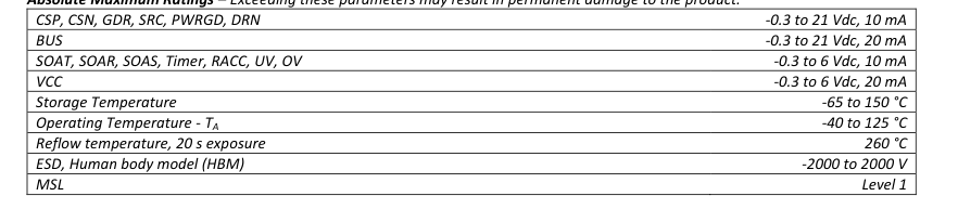
Recommended Electrical Specifications
| Parameter | Notes | Min | Typ | Max | Units |
|---|---|---|---|---|---|
| Junction Temperature | -40 | 125 | °C | ||
| SRC, DRN, CSP, CSN | 14 | Vdc | |||
| BUS | 0.9 | 14 | Vdc | ||
| VCC capacitor | VCC bypass capacitor | 1 | 10 | µF |
Electrical Specifications Unless otherwise specified: -40C < TJ < 125C, BUS > 4.5 to 14 Volts (No Auxiliary Supply at VCC), BUS = 0.9 to 4.5 Volts ( 3.8 V < VCC < VCC Clamp). RACC = 20.0k
| Parameter | Min | Typ | Max | Units | Conditions |
|---|---|---|---|---|---|
| VCC Supplied from VAUX using RAUX (1). (BUS = 0.9 to 4.5 V) | |||||
| VAUX Range (with series RAUX) | 4.5 | 14.0 | V | Required for BUS = 0.9 to 4.5V | |
| Operating Icc | 7 | 13 | mA | UV/EN pin enabled | |
| Standby Icc | 6 | 12 | mA | UV/EN pin disabled | |
| Vcc Clamp | 4.5 | 5.2 | V | Operating I range CC | |
| VCC derived from BUS (BUS = 4.5 to 14 Volts, No VAUX Supply) | |||||
| Operating I from BUS pin CC | 8 | mA | UV/EN pin enabled | ||
| Standby I from BUS pin CC | 40 | 100 | uA | UV/EN pin disabled | |
| POR (VCC derived) | 3.2 | V | |||
| VCC Regulation | 3.8 | 4.3 | V | Operating I range, UV/EN pin CC enabled. | |
| UV/EN and OV | |||||
| Disable Threshold (pin UV/EN) | 0.375 | V | 200us delay after UVLO low trip | ||
| Enable Threshold (pin UV/EN) | 0.575 | V | |||
| Enable Pin Blanking Filter (pin UV/EN) | 100 | 300 | us | ||
| Threshold Hysteresis (pin UV/EN) | 50 | mV | |||
| UVLO Threshold (Low to High Transition of VIN) | 0.725 | 0.75 | 0.775 | V | UVLO De-asserted |
| UVLO Hysteresis | 50 | 75 | 100 | mV | |
Note 1: VAUX is defined on Page 11 and is shown in Figure 6.
Rev 1.1, Page 3 of 26
Page 4
Electrical Specifications(Continued) Unless otherwise specified: -40C < TJ < 125C, BUS = 4.5 to 14 Volts (No Auxiliary Supply at VCC), BUS = 0.9 to 4.5 Volts ( 3.8 V < VCC < VCC Clamp). RACC = 20.0k
| Parameter | Min | Typ | Max | Units | Conditions |
|---|---|---|---|---|---|
| OVLO Threshold (High to Low Transition of VIN) | 0.650 | 0.675 | 0.700 | V | OVLO De-asserted |
| OVLO Hysteresis | 50 | 75 | 100 | mV | |
| UVLO Blanking Filter | 100 | 300 | us | ||
| OVLO Blanking Filter | 5 | 10 | 15 | us | |
| UVLO/OVLO Holdoff Time | 100 | 300 | us | Ensures gate is maintained low. | |
| OV Current | -0.3 | 0.3 | uA | ||
| UV Current | -0.3 | 0.3 | uA | ||
| Gate Drive (V @ GDR pin to GND, V @ GDR pin to SRC pin). Operation is not in Current Limit. GATE GS | |||||
| V High GATE | V + BUS 4.65 | V + BUS 6.5 | V | Not to exceed 21V. | |
| Gate Drive Operating Range (V ) GS | 4.65 | 6.5 | V | ||
| V Current Limit Disable Threshold GS | 4.0 | 4.6 | V | Power Good | |
| V Current Limit Enable Threshold GS | 0 | 1 | V | Start-up | |
| Gate Current (Sourcing Mode) | 10 | 40 | uA | V = 0 to 4.6 V GS | |
| Gate Current (Sinking Mode) (2) | 0.18 | 0.25 | 0.33 | mA | V = 0.3 to Gate Drive Operating GS Range. V > Drain Low-Threshold DRAIN |
| Gate Current (Sinking Mode) (2) | 4 | 8 | 16 | mA | V = 14 V. GATE V < Drain High-Threshold DRAIN |
| OFF State Gate Discharge Path to GND (Gate Pull Down) | 30 | Ohm | @ 50 mA | ||
| SRC Pin Current | -2 | 2.5 | uA | @ 14 Volts. Positive Current into pin. | |
| Current Limit & Sense (CSP to CSN) | |||||
| Differential Current Limit Sense Voltage | 21 | 25 | 27 | mV | T = 25°C A |
| Current Ramp Time to Current Limit Level (GBD) | 30 | 120 | us | Settling to within 5% | |
| Current Limit Overshoot (GBD) | 10 | % | Closed loop, shorted load, MOSFET transconductance 20 to 200 A / V | ||
| CSP Pin Current | -10 | 10 | uA | ||
| CSN Pin Current | -10 | 10 | uA | ||
Note 2: This current is the gate discharge current for all shutdown conditions except circuit breaker (short circuit). This includes UV, Disable (UV/EN pin), OV, SOA.
Rev 1.1, Page 4 of 26
Page 5
Electrical Specifications(Continued) Unless otherwise specified: -40C < TJ < 125C, BUS = 4.5 to 14 Volts (No Auxiliary Supply at VCC), BUS = 0.9 to 4.5 Volts ( 3.8 V < VCC < VCC Clamp). RACC = 20.0k
| Parameter | Min | Typ | Max | Units | Conditions |
|---|---|---|---|---|---|
| Circuit Breaker (CB) (CSP to CSN), Refer to Figure 9 Timing Diagram | |||||
| Differential Circuit Breaker Trip Sense Threshold (3) | 47 | 52 | 57 | mV | T = 25°C A |
| Circuit Breaker Sense CMRR | 65 | 80 | dB | 50KHz @ T = 25°C A | |
| Circuit Breaker Detection Delay | 100 | 150 | ns | CB event to 99% V . 3 mV overdrive GS (above trip point). | |
| Gate High Discharge Current (Stage 1 shutdown) | 40 | 80 | 160 | mA | V = 14 V GATE |
| Gate Intermediate Discharge Current (Stage 2 shutdown) | 4 | 8 | 16 | mA | V = 14 V GATE V < Drain High-Threshold DRAIN |
| Gate Low Discharge Current (Stage 3 shutdown) | 0.18 | 0.25 | 0.33 | mA | V = 0.3 to Gate Drive Operating GS Range. V > Drain High-Threshold DRAIN |
| Drain Low-Threshold (ΔV ) DRN | 2 | Positive differential change in V DRN during CB shut-down. Discharge goes from Stage 1 to Stage 2. | |||
| Drain High-Threshold (V ) DRN | 14 | 15 | 16 | V | Positive going drain voltage threshold (gate discharge transitions from Intermediate to Low Current) |
| Drain High-Threshold Hysteresis | 0.9 | V | Negative going drain voltage threshold minus Positive going threshold | ||
| Response Time 1 | 5 | ns | Drain Low-Threshold to Gate Intermediate Discharge Current (settled within 5%) | ||
| Response Time 2 | 30 | ns | Drain High-Threshold to Gate Low Discharge Current (settled within 5%) | ||
| Circuit Breaker Trip Hold Time | 100 | 300 | us | Gate maintained low | |
Note 3: The Circuit Breaker fault is enabled only when no other fault has occurred prior to exceeding the 52mV threshold. If another shutdown event occurs first (SOA shutdown, UV shutdown, OV shutdown, Disable shutdown) then circuit breaker fault sensing is disabled and held disabled until the gate is fully discharged and the trip hold time has passed. See Figure 9 for details.
Rev 1.1, Page 5 of 26
Page 6
Electrical Specifications Unless otherwise specified: -40C < TJ < 125C, BUS = 4.5 to 14 Volts (No Auxiliary Supply at VCC), BUS = 0.9 to 4.5 Volts ( 4.2 V < VCC < VCC Clamp). RACC = 20.0k
| Parameter | Min | Typ | Max | Units | Conditions |
|---|---|---|---|---|---|
| SOA | |||||
| Differential Current Sense Level Range for SOA (CSP to CSN) | 0 | 80 | mV | ||
| SOAS | |||||
| SOAS Current Scaling Factor (R * R ) SENSE SOAS | 10 | Ω2 | This is the means to scale current for SOA. | ||
| R Resistor Range (SOA Note 1) SOAS | 1 | 20 | kΩ | RACC resistor 20 K. | |
| V range (CSN to SRC), Active SOA DS | V DS min | VBUS | V | ||
| Minimum V Sense Level to enable SOA Shutdown DS | 23 | 33 | mV | Below this level SOA shutdown is disabled. | |
| SOAR | |||||
| Rth Range jc | 0.38 | 7.5 | oC/W | Range for exposed pad MOSFETs | |
| SOAR to Rth Conversion Factor jc | 0.38 | oC/(W∙kΩ) | RACC resistor 20 K. | ||
| R Resistor Range (SOA Note 1) SOAR | 1 | 20 | kΩ | RACC resistor 20 K. | |
| Rth ca | 60 | 60 | 60 | oC/W | Value Fixed Digitally |
| SOA Shaper 2 Input Range (V * I * Rth ), DS ca | 4800 | Units | One unit = 1 V * 1 A *1 oC/W, SOA Note 1 | ||
| SOA Update Rate (Time from A/D Acquisition of V DS & I to Update of Digital Filter) | 13.5 | 15 | 16.5 | us | Includes all A/D conversions, and all multiplications. |
| SOAT | |||||
| SOA Shaper 1: Tau Range p | 0.96 | 19.27 | ms | SOA Note 2 | |
| SOAT to Tau Conversion Factor p | 19.27 | kΩ ∙ ms | RACC resistor 20 K. | ||
| R Resistor Range SOAT | 1.3 | 20 | kΩ | ||
| SOA Shaper 1: (Tau / Tau ) Ratio z p | 1/8 | 1/8 | 1/8 | SOA Note 2 | |
| SOA Shaper 2: Tau | 1.8 | 2 | 2.2 | sec | SOA Note 2 |
| A/D Anti-Aliasing Filter 3 dB | 3.3 | 13 | KHz | GBD – Not tested in production | |
| SOA Comparator Input Resolution | 1.19 | °C | |||
| SOA Comparator Hi Threshold | 60 | °C | All SOA cycles | ||
| SOA Comparator Lo Threshold | 21 | °C | First 16 SOA cycles. | ||
| SOA Comparator Lo Threshold | 3 | °C | Beyond 16 SOA cycles. | ||
SOA Note 1: Recommended minimum resistor value is 1.30k SOA Note 2: SOA Shaper 1 has a function that is represented by a normalized step response of the form:
[
]
SOA Shaper 2 is represented by a normalized step response of the form:
See "Junction to Case Thermal Response" section for further details.
Rev 1.1, Page 6 of 26
Page 7
Electrical Specifications Unless otherwise specified: -40C < TJ < 125C, BUS = 4.5 to 14 Volts (No Auxiliary Supply at VCC), BUS = 0.9 to 4.5 Volts ( 3.8 V < VCC < VCC Clamp). RACC = 20.0k
| Parameter | Min | Typ | Max | Units | Conditions |
|---|---|---|---|---|---|
| Power Good (PWRGD) | |||||
| PWRGD Voltage (Output De-asserted) | 0.4 | V | @5mA | ||
| PWRGD Current (Output Asserted) | 0 | 2 | uA | @ V = 14 Volts, VBUS = 0.9 to 14 Volts | |
| PWRGD Current (Output Asserted) | 0 | 2 | uA | @ V= 0.9 Volts, VBUS=0.9 to 14 Volts | |
| PWRGD during Power Up (GDR Off) | 0.4 | V | @ 2 mA | ||
| V CLDT Event to PWRGD High Prop Delay GS | 1 | us | |||
| V CLET Event to PWRGD Low Prop Delay GS | 1 | us | |||
| Timer | |||||
| Rtimer Resistance Range | 1 | 20 | k | Resistance at Timer Pin. RACC resistor 20 K. | |
| Rtimer to Time Conversion Factor | 5 | ms / k | RACC resistor 20 K. | ||
| Hot Swap Initialization Time | 5 | 100 | ms | RACC resistor 20 K. | |
| Hot Swap Initialization Time Error | -25 | 25 | % | RTimer resistor 1.25 K to 20 K. | |
| Thermal Resistance | |||||
| Rθ J-A | 46 | °C/W | TAB connected to copper PCB trace. | ||
Rev 1.1, Page 7 of 26
Page 8
PI2211 Introduction
The PI2211 limits the start-up current to a load, eliminating the electrical disturbance or possible voltage sag imposed on a backplane power supply. The PI2211 performs hot swap protection during power-up or insertion and acts as a circuit breaker during steady state operation. The PI2211 performs these protection functions by controlling an external MOSFET and limiting the MOSFET junction temperature rise to a safe level, a key requirement for hot swap power managers expected to operate over wide dynamic conditions.
Upon insertion, the PI2211 initiates a user programmable turn-on delay where the gate of the MOSFET is held "off", providing input BUS de-bounce. The PI2211 then turns "on" the MOSFET pass element in a controlled manner, limiting the current to a pre-defined level based on the value of a user selected sense resistor. The PI2211 circuit breaker threshold protects against over-current by comparing the voltage drop across this sense resistor with a fixed internal reference voltage. Once the load voltage has reached its steady-state value, the Power-good pin is asserted "high" and the start-up current limit is disabled. Under voltage (UV) and Over Voltage (OV) trip points (user settable) ensure operation within a
defined operating range in addition to a Enable/Disable feature shared with the UV input.
With Power-good established, the load current is continuously monitored by the PI2211 with the MOSFET operating in the low loss RDSON region. In this steady state operation, the PI2211 now acts primarily as a circuit breaker. An over-current threshold is fixed to be twice the start-up current limit and sets an upper current boundary that determines when a gross fault has occurred. Exceeding this boundary will initiate the PI2211 Glitch-Catcher™ circuitry and assert the power good pin low.
Glitch-Catcher™ The Glitch-Catcher™ feature of the PI2211 prevents overvoltage events caused by the energy stored in the parasitic inductance of the input power path in response to a rapid interruption of the forward current during an overcurrent fault event. Acting as an active snubber, this circuitry mitigates the need for large external protection components by shunting the energy through the MOSFET to the low impedance load.
True-SOA™ The Picor PI2211 ensures efficient operation within the MOSFET SOA by emulating the MOSFET junction temperature rise via a internal digital processor. The PI2211, with True- SOA™, constantly monitors MOSFET power to calculate the MOSFET junction temperature rise and determine the proper operation regardless of load conditions. The amount of time that the PI2211 will turn a MOSFET on during SOA is dependent on the calculated temperature rise, not a fixed time, making the pulse width dynamic with varying line voltages. The PI2211 will keep the MOSFET on until it predicts an absolute 60°C junction temperature rise. Selecting 60°C as the maximum junction temperature rise allows for the use of
the MOSFET at ambient temperatures approaching 90°C and prevents exceeding the MOSFET’s maximum junction temperature, typically at 150°C.
Once the junction temperature rise has been calculated to be 60°C, the PI2211 will shut down the MOSFET and allow for thermal cooling. While in True-SOA™ protection mode, the PI2211 will attempt to start the MOSFET when the True- SOA™ emulator has calculated that the junction temperature has dropped by 39°C. The 39°C thermal cycling range will retry start-up for a total of 16 pulses before the range is extended to 57°C, where the thermal cycling will go on indefinitely or until the low impedance load is removed.
The PI2211 can also protect the MOSFET when it is operating at a higher than anticipated load current, but still below the circuit breaker threshold. True-SOA™ constantly calculates junction temperature rise as a function of power dissipation and can shut down the MOSFET preventing damage. A typical hot-swap controller will only fault when a threshold is exceeded and cannot continuously protect the MOSFET during operation.
Emulation of the MOSFET thermal performance is possible with the use of the MOSFET manufacturers’ transient thermal impedance curves. The Picor True-SOA™ digital algorithm ensures maintaining a MOSFET within the actual SOA of the device, optimizing the size of the device without the need to oversize the MOSFET. The PI2211 True-SOA™ is programmed for specific MOSFET thermal characteristics by the setting of three resistors. The SOAS resistor determines the magnitude and scaling of the current through the MOSFET. The SOAR and SOAT resistors program the transient thermal parameters of the MOSFET's junction to case characteristics. By programming the MOSFET thermal characteristics, the PI2211
adapts its control and start-up or thermal cycling to that specific MOSFET as shown in Figure 5.
Rev 1.1, Page 8 of 26
Page 9
PI2211 Application/Theory of Operation
Maintaining a MOSFET within its SOA boundary: The PI2211 has a programmable digital model of a MOSFET thermal response to transient and static loads that it uses to predict a junction temperature rise, as a function of power, for a given MOSFET. The equivalent analog model is shown in Figure 2. It consists of two RC stages to emulate the total thermal equivalent of the junction-to-case and case-to- ambient characteristics of the MOSFET and its package. In the model, the case-to-ambient characteristics are fixed while the junction-to-case can be tuned to match the published data for a specific MOSFET by two programming resistors; RSOAT and RSOAR.
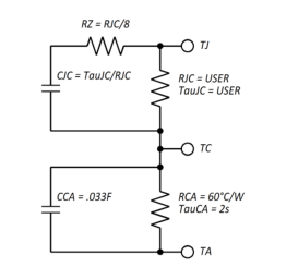
Figure 2 - Simplified representation of the PI2211 thermal
model.
The RSOAT resistor controls the time constant (TauP) of the SOA junction-to-case model. This resistor programs the model to adhere to the manufacturer’s transient thermal impedance graph of the junction-to-case response to "single pulse" power changes, as well as the extended SOA curves beyond the DC area limit. This instantaneous power calculation refreshes in less than 50µs and predicts junction temperature rise within the 1ms extended SOA MOSFET curves so the PI2211 will protect the MOSFET from prolonged heating with excessive static loads and hot-spotting from transient loads.
The RSOAR resistor programs the model with the RJ-C of the MOSFET. Scaled by the ratio of the junction-to-case/case-to- ambient thermal impedances (RJ-C/RC-A), referenced to the fixed internal 60°C/W RC-A of the PI2211.
The RSOAS resistor programs the magnitude of the calculated current through the MOSFET and the power it is dissipating. All three of these resistors have a maximum value 20kΩ and a 1.30kΩ minimum value. Values outside of these ranges will not stop the PI2211 from working, but will force the internal references to either their minimum or maximum values. See the Recommended Design Steps section for more details on calculating the required SOA programming resistors.
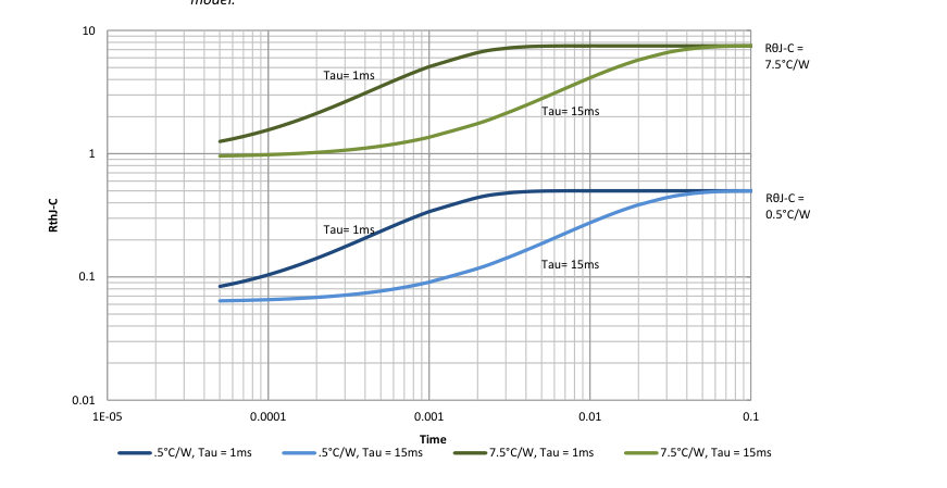
Figure 3 - The range of PI2211 RθJ-C thermal impedance adjustment at 1W.
Rev 1.1, Page 9 of 26
Page 10
Junction-to-Case Thermal Response: The magnitude of the MOSFET junction-to-case temperature rise is the product of the MOSFET junction-to-case thermal resistance (RJ-C), the sampled instantaneous power dissipated in the MOSFET and the duration of the power dissipation. The PI2211 internal model of RJ-C includes both a “pole” and a “zero” in the transfer function as an electrical equivalent of the thermal resistance and storage components of the MOSFET in the thermal model. The pole, TauP, has a slower response to the dissipated power than the zero TauZ does. TauZ is internally calculated to be 1/8th of TauP. RJ-C and TauP are derived directly from the manufacturer’s
datasheet, and is further explained in the Recommended Design Steps section.
The PI2211 junction-to-case thermal response is shown in Figure 3; bounded by the internal allowed ranges of TauP and RJ-C. The range of TauP is 1ms to 15ms, the range of RJ-C is 0.5°C/W to 7.5°C/W, and the minimum pulse width is 50us. The "Power" term is the calculated power based on the value of RSOAS, which may be scaled from the true power. The response of the PI2211 junction-to-case model is based on the following equation:
[ [
⁄ ] ]
Using the ratios of TauP to TauZ, the equation simplifies to:
[
⁄ ]
The calculated minimum RJ-C is 1/8th of its nominal (steadystate) value, meaning that the PI2211 will predict a higher junction temperature rise than what the manufacturer's curves would suggest for shorter pulse widths. This helps to protect against transient hot-spotting in the MOSFET.
Case-to-Ambient Thermal Response: The magnitude of the MOSFET case-to-ambient temperature rise is a function of the MOSFET case-to-ambient thermal resistance (RC-A) and the instantaneous calculated power dissipated in the MOSFET. The internal model has a “pole” with a fixed thermal time constant (Tau) of 2 seconds and a fixed RC-A of 60°C/W. A 2 second Tau will shut off the MOSFET quickly at power levels that would typically require 100's of seconds to achieve an actual 60°C temperature rise, protecting the MOSFET from thermal stress. 60°C/W is a typical value of RC-A for packages with thermal tabs.
⁄ ]
[
Junction-to-Ambient Thermal Response: The over-all range of the junction-to-ambient thermal impedance response of the PI2211 is shown in Figure 4. This represents the entire adjustable range of the dynamic RJ-C and the fixed RC-A summed together.
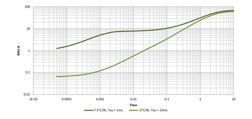
Figure 4 - PI2211 J-A Thermal Impedance range of adjustment at 1W.
Rev 1.1, Page 10 of 26
Page 11
SOA Thermal Cycling: The PI2211 continuously monitors the power dissipation in the MOSFET by measuring the voltage drop across the MOSFET (VDS) and the calculated current through the sense resistor (IDRAIN). As previously described the power information is processed through two equivalent internal networks whose individual responses emulate the MOSFET RJ-C and RC-A thermal characteristics. These two responses are summed together to create an accurate RJ-A thermal response.
When the computed junction temperature rise in the MOSFET is 60°C, the MOSFET is turned off and, while still being continuously monitored, allowed to cool to a calculated junction temperature rise of 21°C (an estimated drop of 39°C). The MOSFET is once again turned on and monitored. The PI2211 will continue the thermal cycling of the MOSFET 16 times with this temperature hysteresis range before dropping the cool down temperature to 3°C rise. Once at 3°C, the PI2211 will continue the thermal cycling indefinitely with a 57°C temperature hysteresis range resulting in a long cool down period. An example of this SOA thermal cycling is shown below in Figure 5 and in Figure 11.
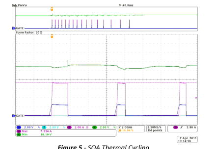
Figure 5 - SOA Thermal Cycling
Figure 5 shows the initial string of 16 SOA pulses. The VGS is displayed on Ch1 (blue), the start-up current is shown on Ch3 (purple) and the BUS voltage is shown on Ch4 (green). Power -good is shown on Ch2 (light blue), which is low during SOA.
VAUX Supply/Gate Drive: The PI2211 is designed to be used in systems where the BUS voltage range is from 0.9Vdc to 14Vdc. When using a BUS voltage of 4.5Vdc or greater, the PI2211 internal LDO regulator creates a VCC voltage of 4Vdc to bias the IC.
When using a BUS of less than 4.5Vdc, an external supply (VAUX) is required to drive VCC; typically 5Vdc or greater with
a series current limiting resistor (RAUX), as is shown in Figure 6, to protect the internal clamp of the VCC pin. The RAUX limiting resistor is calculated as: RAUX = (VAUX - 3.8V)/10mA. Though the BUS pin is not used to generate VCC, it still must be connected to the BUS supply for proper operation.
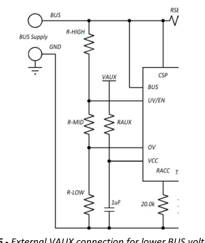
Figure 6 - External VAUX connection for lower BUS voltages.
The PI2211 has an internal charge pump that requires no external components and is designed to be used with MOSFET that can operate with a gate drive of 4.5Vdc.
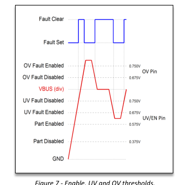
Figure 7 - Enable, UV and OV thresholds.
Rev 1.1, Page 11 of 26
Page 12
UV/EN and OV: Figure 7 depicts the divided down BUS voltage, monitored on the UV/EN and OV pins respectively and the "fault" state of the PI2211. The over-voltage (OV) pin will disable (fault) the PI2211 once the voltage on the OV pin reaches 0.750Vdc. It will re-enable (fault clear) the controller once the voltage drops below 0.675Vdc.
The UV/EN pin monitors for under-voltage faults and also provides a means of disabling the part via an external control. The part becomes enabled once the voltage on the UV/EN pin exceeds 0.575Vdc. To disable the part, the voltage on the UV/EN pin must be below 0.375Vdc. A UV fault occurs when the voltage on the UV/EN pin drops below 0.675Vdc, disabling the controller. The fault is cleared and the controller re-enabled, when the UV/EN pin’s voltage exceeds 0.75Vdc.
Glitch-less Turn-off: Transient Turnoff Glitch-Catcher™ During a circuit breaker event, uncontrolled turn off of the series MOSFET can cause voltage ringing on the BUS due to the stored energy in components and copper traces. To maintain BUS voltage stability the PI2211 uses a glitch-less turn-off mechanism whereby the MOSFET gate is initially
discharged rapidly, then in a slower controlled discharged to a full "off" state. This allows the stored energy to pass through the MOSFET into the low impedance load, keeping the BUS voltage ringing to a controlled maximum value, well below the avalanche voltage rating of the MOSFET. Acting as an active snubber this provides the same protection as having a voltage suppressor on the BUS. Figure 8 shows a simplified block diagram of the Glitch-Catcher™ circuit.
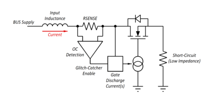
Figure 8 - Glitch-Catcher™ Over-current fault detection circuit.
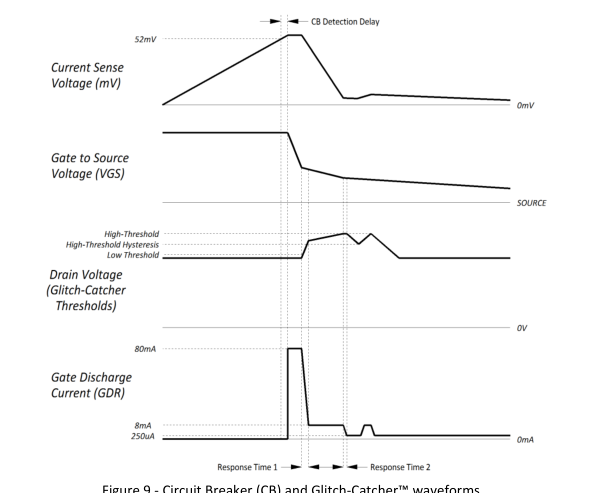
Figure 9 - Circuit Breaker (CB) and Glitch-Catcher™ waveforms.
Figure 9 represents the typical response waveforms of the
with an 80mA discharge current until there is a positive dv/dt
PI2211 Glitch-Catcher™ to a circuit breaker (CB) event. After
on the drain. The discharge current is reduced to 8mA which
the CB detection delay, the MOSFET gate gets discharged
slows the drain voltage over-shoot until the drain - high
Rev 1.1, Page 12 of 26
Page 13
threshold limit is passed. The discharge current is again reduced to 250uA to slowly discharge the MOSFET gate. As the drain voltage falls below the hysteresis threshold of the drain-high threshold, the discharge current is increased to 8mA. This hysteretic cycling of discharge currents continues until the gate is completely discharged.
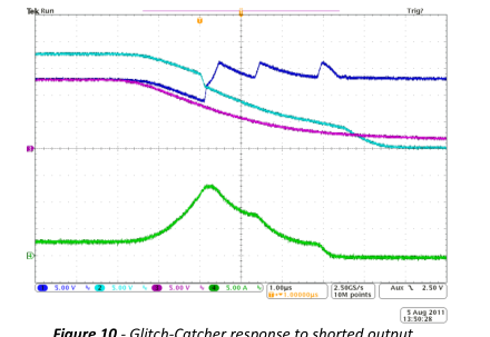
Figure 10 - Glitch-Catcher response to shorted output.
Figure 10 shows the Glitch-Catcher™ responding to a hard short-circuit applied to its output. The BUS voltage (blue, Ch1) starts to drop as the current though the FET (green, Ch4) rises. The source voltage (purple, Ch3) separates from the BUS voltage as the voltage drop across the sense resistor and the FET increases. The gate voltage (cyan, Ch2) tracks the BUS voltage until the over-current threshold is exceeded, which starts the Glitch-Catcher™ controlled gate discharge circuitry.
Current Limit: The PI2211 has a start-up current limit and a circuit breaker threshold, as shown in Figure 11. The designer’s MOSFET selection can be determined by the maximum load current, acceptable power loss at max current and the maximum ambient temperature.
The PI2211 has a current sense amplifier that uses an external current sense resistor to monitor MOSFET current. The circuit breaker current threshold is determined by dividing the internal 52mV reference voltage by the desired over-current threshold. Exceeding this threshold will initiate the Glitch-Catcher™ shut-down function, but the current is not restricted. Since sense resistor value increments are limited an additional resistor divider might be needed to adjust for the desired circuit breaker threshold.
The start-up current level is set to approximately half the circuit breaker threshold; (0.025V/0.052V) \* circuit breaker current. The start-up current limit is only in effect during start-up, while the power-good signal is low, and acts to limit the amount of current that the load can draw.
When start-up is completed, and power good is asserted high, the current limit is no longer enabled and the circuit will be allowed to draw current up to the circuit breaker threshold or until an SOA fault is calculated. The circuit breaker threshold is always enabled.
Another current threshold to consider is the maximum operating current, IDCMAX. IDCMAX is calculated based on the maximum rated junction temperature and the thermal and resistive properties of the MOSFET. See the IDCMAX equation in the Recommended Design Steps section for more details. Operating above this current will result in an SOA shut down and thermal cycling of the MOSFET when the PI2211 is properly programmed.
The waveforms in Figure 11 are representative of a typical start-up sequence, followed by an over-current event, and then a re-start into a shorted load, leading to SOA thermal cycling.
As the BUS supply rises and clears the VCC POR and UV fault thresholds, the programmable insertion delay timer starts. After the insertion delay, the series MOSFET gate is charged with a 25uA current, allowing the input current to gradually increase until it reaches the start-up current threshold. The gate will be regulated to maintain the start-up current until either the output reaches the BUS voltage or the MOSFET is turned off due to SOA. Here, the output voltage reaches the BUS voltage and the current drops below the start-up current threshold, stopping the regulation of the MOSFET VGS and allowing it to increase to the full charge pump voltage level of
about 5V. The power good pin is de-asserted and allowed to float once the VGS is above 4.4V.
Sometime after the normal start-up an over-current event occurs, triggering the Glitch-Catcher™ turn-off of the MOSFET and the low assertion of the power good pin. See Figure 9 for further details.
Rev 1.1, Page 13 of 26
Page 14
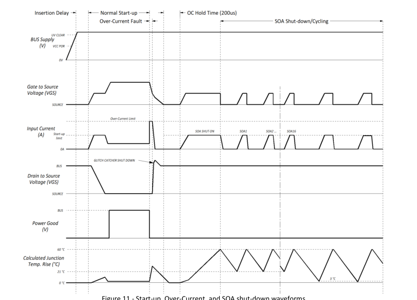
Figure 11 - Start-up, Over-Current, and SOA shut-down waveforms.
The MOSFET is held off for 200us before attempting to re- start. Again, the MOSFET will be regulated to the start-up current level, but now turns off due to an SOA shut-down. The True-SOA™ protection has determined that the junction temperature of the MOSFET has risen by 60°C and has shut it down to cool. When the SOA monitoring has determined that
the junction temperature has dropped by 39°C the MOSFET will again turn on. The 39°C thermal cycling range will continue for a total of 16 pulses before the range is extended to 57°C, where the thermal cycling will go on indefinitely until the low impedance load is removed.
Rev 1.1, Page 14 of 26
Page 15
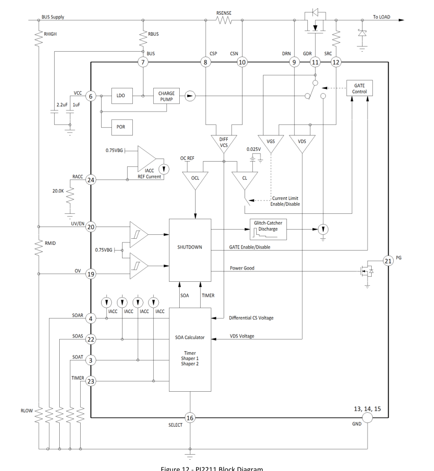
Figure 12 - PI2211 Block Diagram.
Rev 1.1, Page 15 of 26
Page 16
PI2211: Recommended Design Steps
There are two options to designing a hot swap solution with the PI2211: Utilize PICOR's PI2211 reference design with pre-selected components Follow PICOR's design guidelines and use the "Picor Calculator Tool" available from Picor's website
Either of these approaches will yield a suitable and reliable hot swap design solution.
PICOR PI2211 Reference Design:
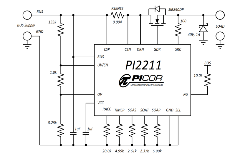
Figure 13 - Final Design Schematic
For this design example we'll define our system requirements as follows: Nominal BUS voltage (VBUS) = 12V High BUS voltage where controller must be enabled (VBUSHIGH) = 12.5V Low BUS voltage where controller must be enabled (VBUSLOW) = 11.5V Maximum Operating Current (IMAX) = 10A Circuit Breaker Threshold (ICB) = 13A Hot-Swap Efficiency > 99% Schottky Diode is 40V, 1A; required to protect the SCR pin from negative voltage transients that can damage the controller. The 100Ω series resistor is used to limit current.
Rev 1.1, Page 16 of 26
Page 17
Design Example FET Table: In the preceding design Vishay's SiR890DP was used for the series MOSFET. The following table lists suitable MOSFETs and their associated component values for use in various design configurations.
| VBUS | IMAX | ICB | RSENSE | MOSFET | Manufacturer | RSOAR | RSOAS | RSOAT | PULSE |
|---|---|---|---|---|---|---|---|---|---|
| 12V | 22A | 26A | 0.002Ω | IRFH5300PbF | IR | 2.32k | 2.67k | 1.74k | 8ms |
| IRFH6200PbF | IR | 2.32k | 2.67k | 2.26k | 7ms | ||||
| 10A | 13A | 0.004Ω | BSC019N02KSG | Infineon | 4.32k | 1.69k | 1.74k | 8ms | |
| FDMS7570S | Fairchild | 4.87k | 1.87k | 2.15k | 5ms | ||||
| SiR890DP | Vishay | 5.90k | 2.61k | 2.37k | 2ms | ||||
| IRFH5300PbF | IR | 2.32k | 1.33k | 2.74k | 22ms | ||||
| 5V | 10A | 13A | 0.004Ω | BSC019N02KSG | Infineon | 4.32k | 1.69k | 2.05k | 41ms |
| SiR890DP | Vishay | 5.90k | 2.61k | 1.96k | 10ms | ||||
| IRFH5304PbF | IR | 13.3k | 1.30k | 1.87k | 11ms | ||||
| 5A | 6.5A | 0.008Ω | SiR890DP | Vishay | 5.90k | 1.30k | 4.02k | 49ms | |
| SiR802DP | Vishay | 10.7k | 1.30k | 1.43k | 20ms | ||||
| BSC046N02KSG | Infineon | 9.76k | 1.30k | 2.26k | 38ms | ||||
| FDMS7580S | Fairchild | 15.8k | 1.30k | 1.96k | 12ms | ||||
| IRFH5304PbF | IR | 13.3k | 1.30k | 1.58k | 20ms |
Table 1 - Reference Design Variations and Associated Components
Rev 1.1, Page 17 of 26
Page 18
PI2211 Design Guidelines
Table 1 lists some typical system configurations; their N- MOSFETs and associated PI2211 programming resistors. There are 9 different MOSFETs listed from various manufacturers; all in the 5 x 6mm power tabbed package.
When designing a system that is not captured by the reference designs listed in Table 1, the recommended design steps are as follows: 1) Determine the value and power rating of the current sense resistor (RSENSE) based on the maximum allowed current where a circuit breaker fault event will be set. 2) Determine the maximum RDSON and RθJ-A that the system can tolerate for a 60°C delta rise in junction temperature to chose an appropriate MOSFET. 3) Calculate the required programming resistors of the PI2211 based on the system requirements and the selected MOSFET. 4) Calculate the under and over-voltage resistors, based on the required window of operation of the
BUS voltage.
Component values for the PI2211 can be taken directly from the reference design examples, by using the equations in this datasheet, or by using the Windows® based component calculator software for the PI2211.
1) Sense Resistor Calculation: The value of the current sense resistor, RSENSE, determines the start-up current limit and circuit breaker threshold. During start-up, the PI2211 will actively regulate at the start-up current limit, which is calculated as follows:
Where; 0.025V is the internal reference voltage for the startup current to the sense comparator.
The circuit breaker threshold, ICB, is approximately twice the ISTART-UP current. When designing a system using the PI2211, it is often better to determine the maximum over-current threshold that the design can tolerate rather than the startup current, since during start-up the MOSFET is protected by the PI2211 SOA capabilities.
Where; 0.052V is the internal reference voltage for circuit breaker threshold to the sense comparator.
The power rating of RSENSE should calculated to be about double that of the power dissipated at the over-current level.
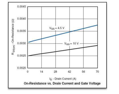
2) Maximum RDSON and RθJ-A Calculation: The product of the constant power across the MOSFET and the junction to ambient thermal resistance (RθJ-A) must be less than 60°C. The power across the MOSFET is the product of the square of the maximum operating current and the RDSON, multiplied by the RDSON thermal scalar at 150°C, which is typically about 1.6.
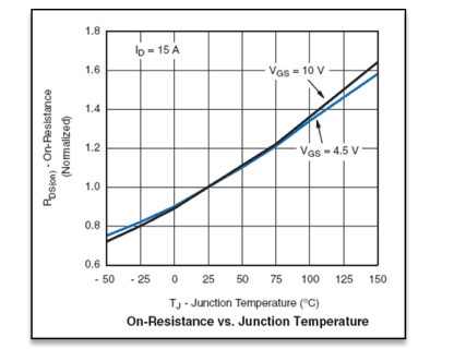
Figure 14 - Examples of an RDSON (left) and a RDSSCALAR thermal scalar (right) graphs.
Rev 1.1, Page 18 of 26
Page 19
RDSON and RDSSCALAR Using the VGS @ 4.5V trace, the RDSON can be taken from the graph on the left in Figure 14, using the desired operating current as an X intercept. Once that value is chosen, the graph on the right will determine the scalar of the RDSON value at the maximum junction temperature. In this example it is about 1.58X, also taken using the VGS @ 4.5V trace.
IDCMAX is the DC operating current that will heat the MOSFET to its maximum junction temperature TJMAX when the surrounding environment is at some maximum ambient temperature. It is found by taking the maximum allowed temperature rise of the MOSFET, based on the difference between the maximum MOSFET junction temperature and the maximum ambient temperature, and dividing this by the thermal resistance of the MOSFET, RJ-A. The results will be the maximum wattage (power) of the MOSFET. Dividing this wattage by the RDSON of the MOSFET, at its maximum junction temperature, will yield the maximum operating current squared. IDCMAX is calculated as 90% of this value.
√
Where; TJMAX = Maximum allowed junction temperature TAMBMAX = Maximum ambient temperature RDSON = The MOSFET "On" resistance @ room temperature. RDSSCALAR = The MOSFET "On" resistance multiplier @ the maximum junction temperature. RJA = The MOSFET thermal resistance, junction to ambient.
Recommended MOSFETs: The ability to program the PI2211 to maintain a MOSFET in its thermal SOA region allows for a wider selection of MOSFETs to be used in a hot-swap application.
When selecting a MOSFET, the key features to look for are: low RDSON at 4.5VGS a minimum VDS voltage rating of 20V a RθJ-C between 0.5°C/W and 7.5°C/W the peak pulsed current rating packages with metal thermal tabs
The PI2211 is designed to be used with a wide range of MOSFETs in various packages, but to realize the greatest efficiency Picor recommends the use of surface mount MOSFETs with a metal drain tab for the best thermal and RDSon performance. Packages such as Vishay's PowerPAK SO8 and 1212-8, Infineon's PG-TDSON-8 and PG-TSDSON-8, IR's 5 x 6 mm and 3 x 3 mm PQFN, and other similar tabbed packages offer MOSFETs with high current ratings, better
RθJ-C thermal transfer properties and lower RDSon resistances.
3) PI2211 Resistor Calculations: RACC is the resistor used to program the internal current source. Its value is always 20.0k and should be set using a 1% tolerance resistor. The power through the resistor is about 30µW.
RTIMER is the resistor that programs the start-up delay timer after board insertion; DELAY is in the range of 5ms to 100ms. For a 25ms delay:
SOA Programming Components: Every MOSFET has its own unique thermal characteristics, due to die size, lead frame, packaging, etc., and these characteristics need to be "programmed" into the PI2211 digital model for it to accurately emulate and predict the junction temperature rise for any given MOSFET. The model needs to know the MOSFET junction-to-case and junction-to- ambient thermal impedances, as well as the power through the MOSFET, in order to accurately predict the MOSFET junction temperature rise. These unique MOSFET characteristics are used in conjunction with some built-in default model parameters to accurately model a MOSFET in the end user's application.
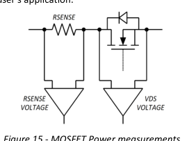
Figure 15 - MOSFET Power measurements.
RSOAS
The PI2211 determines the power across the MOSFET by measuring the voltage drops across the MOSFET and the sense resistor, as is shown in Figure 15. The RSOAS resistor is used to program the PI2211 with the sense resistor's value. The value range of this programming resistor is 1k minimum, to 20k maximum.
The equation for calculating RSOAS is:
[
] [ ] []
Where; 10Ω2 is the SOAS current scaling factor, the default case-to-ambient, RΘCA-DEFAULT, is 60°C/W, the default temperature rise, ΔTDEFAULT, is 60°C,
Rev 1.1, Page 19 of 26
Page 20
the difference between the max junction and the max ambient temperatures is ΔTUSER .
The additional terms for temperature rise and case-to- ambient ratios will scale the RSOAS resistor value, allowing for the fine tuning of the PI2211 digital model to the MOSFET.
For example, if the steady-state RθC-A of the MOSFET is less than the default 60°C/W of the model, the value of RSOAS would be scaled down by this ratio. This would make the value of the sense resistor appear to be larger to the PI2211. For a given voltage drop across the sense resistor, a larger sense resistor value would mean less apparent current flowing through it and therefore the calculated power across the MOSFET is less. By scaling the apparent power a wide range of MOSFETs can be accurately emulated by the digital thermal model.
Similarly, if the user has a lower ΔT than the default, the net result is that the value of the sense resistor appears to be lower, therefore the current flowing through it appears to be greater to the SOA model and it will calculate more power across the MOSFET.
The scaled value of current used to determine RSOAS is used to calculate the power across the MOSFET when calculating TauP and in determining the value of RSOAT.
RSOAT , RSOAR
The PI2211 thermal model has a default case-to-ambient thermal impedance of 60°C/W, and a Tau of 2 seconds. The junction-to-case thermal impedance and
TauP are
programmed by the RSOAT and RSOAR resistors. These can have a maximum value of 20.0k and a minimum value of 1.30k.
RSOAR programs the PI2211 with the junction-to-case (RθJ-C) thermal impedance of the selected MOSFET. The ratio of the internal RθC-A (60°C/W) and the user's RθC-A is used to scale the MOSFET RθJ-C in order to maintain the correct RθJ-C to RθC- A ratio.
[
]
Where; 0.38 °C/(W∙k) is the SOAR to RθJ-C scaling factor, the default case-to-ambient, RθCA-DEFAULT, is 60°C/W, RθJA-USER is the steady-state junction-to-ambient value of the MOSFET, taken from the manufacturer's datasheet, RθJC-USER is the maximum junction-to-case value of the MOSFET, taken from the manufacturer's datasheet.
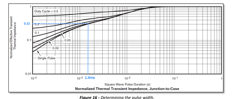
RSOAT programs the PI2211 with the TauP (time constant) of the MOSFET RθJ-C and its value can be calculated after first determining the pulse width that will cause a 60°C temperature rise of the MOSFET junction. This can typically be done using RθJ-C transient thermal impedance curves provided by the FET manufacturer.
The power used for determining the pulse width is the product of the BUS voltage and the start-up current. Multiplying this power by RθJ-C results in a temperature rise. Setting the maximum temperature rise to 60°C for the same power means that the RθJ-C will have to be scaled down. Using this scaling factor and the RθJ-C thermal impedance curves for a single pulse, the pulse width can determined. An example of normalized RθJ-C thermal impedance curves is shown in Figure 16.
Rev 1.1, Page 20 of 26
Page 21
For example: A MOSFET with a RθJ-C of 2.5°C/W, a BUS voltage of 12V, and a start-up current limit of 6.25A will yield the following RθJ-C scaling factor:
Using the thermal impedance curves shown in Figure 16 and a RθJ-C scalar of 0.32, the intersection with the single pulse curve produces a pulse width of 1.4ms. To summarize, a 1.4ms pulse of 75W across this particular MOSFET should raise the junction to case temperature by 60°C.
Knowing the pulse width, TauP can be calculated using the equation below:
[ [
]]
[
]
[
]
Where; PULSE is the pulse width taken from the RθJ-C thermal impedance curves, RθC-A is the default junction to case thermal impedance of 60°C/W, RθJ-C is the maximum junction-to-case value of the MOSFET scaled by the ratio of the FET's RθC-A and the default RθC-A . Power is the nominal BUS voltage multiplied by the current programmed via RSOAS. Power = BUS \* RSOAS \* .0025
The power across the MOSFET is calculated by the PI2211 as the product of the BUS voltage and the programmed current as determined by RSOAS.
Knowing TauP, RSOAT can be calculated using the equation below:
Using junction-to-case thermal impedance curves is a good method to determine the duration of the power pulse since the junction-to-case heats up much faster than the case-to- ambient and they are typically the most accurate thermal curves published.
The MOSFET in Figure 16 reaches its normalized RθJ-C value at about 50ms. MOSFETs with larger die sizes can take much
longer to reach their normalized value, even though they might be in the same package. As this single pulse time increases, then effect of the RθJ-A will become more dominate and the RθJ-A single-pulse thermal impedance curve should be used to determine the pulse width for a 60°C junction rise.
4) Under and Over-Voltage Programming: As is shown in Figure 7, there is a programmable window of BUS voltage range where the PI2211 is guaranteed to be operational. This window is defined by the OV pin voltage being ≤ 0.675Vdc and the UV/EN pin voltage being ≥ 0.750Vdc. The user should be aware that VBUSMAX , when calculated using the following equations, is the maximum voltage where the controller is guaranteed to be operational, not the maximum voltage where the controller faults.
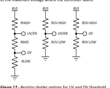
Figure 17 - Resistor divider options for UV and OV threshold
programming.
To calculate the OV and UV resistor divider ratios for separate networks:
Using a three resistor string (RHI, RMID, RLO); when VBUSMIN the voltage on UV is 0.75V, when VBUSMAX the voltage on OV is 0.675V. The ratio of the RMID to RLOW can be determined once the ratio of VBUSMAX to VBUSMIN is set.
Rev 1.1, Page 21 of 26
Page 22
When charging the capacitive load, the required energy peaks at the start of the charging and reduces to zero when the charging is complete. If the energy calculated during the SOA pulse is considered to be the average current, then the peak
Once the max and min BUS voltage has been selected,
energy is twice this amount. The capacitive load can be
plugging their values into these three equations will provide
calculated as:
the resistance ratios of the three resistors.
Optional: Max Load Capacitance Knowing the duration of the power pulse, the user can calculate the available energy during start-up. Knowing this energy, a rough calculation of the amount of load capacitance that can be charged during the initial start-up pulse can be calculated. This calculation takes no tolerances into account.
The energy provided to the load during an SOA pulse is:
PI2211 Design Calculator
The PI2211 component calculator program is designed to calculate the required programming resistors of the PI2211 controller; requiring the designed to enter just a few key thermal MOSFET parameters taken from the manufacturer’s datasheet. It is capable of calculating both an under-voltage/over-voltage divider as well as a current sense divider. It can also derive a usable pulse width when a MOSFET's RθJ-C curves are not given. Please read the PI2211 Component Calculator user guide for instructions on use and available features.
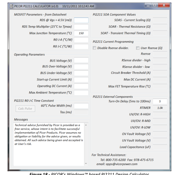
Figure 18 - PICOR's Windows™ based PI2211 Design Calculator
Rev 1.1, Page 22 of 26
Page 23
Mechanicals
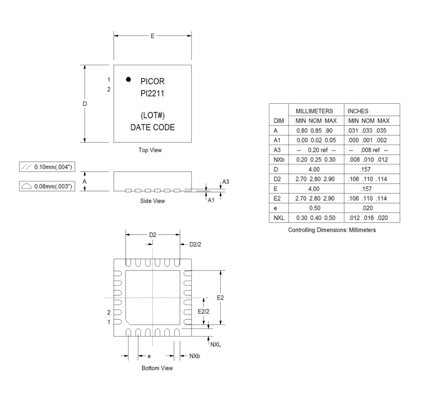
Figure 19 - 24 lead QFN package mechanicals.
Rev 1.1, Page 23 of 26
Page 24
Receiving Pad Definition:
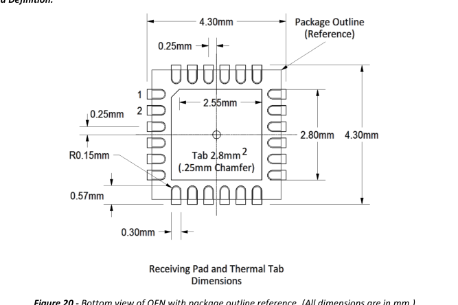
Figure 20 - Bottom view of QFN with package outline reference. (All dimensions are in mm.)
Stencil Definition:
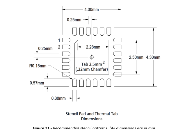
Figure 21 - Recommended stencil patterns. (All dimensions are in mm.)
Stencil definition is based on a 6mil stencil thickness, 80% of LGA pad area coverage.
Rev 1.1, Page 24 of 26
Page 25
PCB Layout Recommendations:
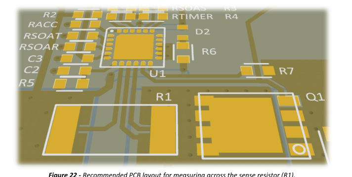
Figure 22 - Recommended PCB layout for measuring across the sense resistor (R1).
PCB Layout The pc board layout shown in Figure 22 is representative of the proper board layout for the most accurate current sensing by the PI2211. The sense line are connected to the internal centers of the sense resistor's pads, minimizing the added resistance of the receiving copper.
Grounding for the PI2211 should be done using either a low current ground plane or a local ground plane, contacting with just the PI2211's ground pins and external components; then connecting this plane to the system ground at a single point. It is not recommended connecting the PI2211's ground pins and external components to different ground planes or to high current ground planes.
Rev 1.1, Page 25 of 26
Page 26
Warranty
Vicor products are guaranteed for two years from date of shipment against defects in material or workmanship when in normal use and service. This warranty does not extend to products subjected to misuse, accident, or improper application or maintenance. Vicor shall not be liable for collateral or consequential damage. This warranty is extended to the original purchaser only.
EXCEPT FOR THE FOREGOING EXPRESS WARRANTY, VICOR MAKES NO WARRANTY, EXPRESS OR LIMITED, INCLUDING, BUT NOT LIMITED TO, THE WARRANTY OF MERCHANTABILITY OR FITNESS FOR A PARTICULAR PURPOSE.
Vicor will repair or replace defective products in accordance with its own best judgment. For service under this warranty, the buyer must contact Vicor to obtain a Return Material Authorization (RMA) number and shipping instructions. Products returned without prior authorization will be returned to the buyer. The buyer will pay all charges incurred in returning the product to the factory. Vicor will pay all reshipment charges if the product was defective within the terms of this warranty.
Information published by Vicor has been carefully checked and is believed to be accurate; however, no responsibility is assumed for inaccuracies. Vicor reserves the right to make changes to any products without further notice to improve reliability, function, or design. Vicor does not assume any liability arising out of the application or use of any product or circuit; neither does it convey any license under its patent rights nor the rights of others. Vicor general policy does not recommend the use of its components in life support applications wherein a failure or malfunction may directly threaten life or injury. Per Vicor Terms and Conditions of Sale, the
user of Vicor components in life support applications assumes all risks of such use and indemnifies Vicor against all damages.
Vicor’s comprehensive line of power solutions includes high density AC-DC and DC-DC modules and accessory components, fully configurable AC-DC and DC-DC power supplies, and complete custom power systems.
Information furnished by Vicor is believed to be accurate and reliable. However, no responsibility is assumed by Vicor for its use. Vicor components are not designed to be used in applications, such as life support systems, wherein a failure or malfunction could result in injury or death. All sales are subject to Vicor’s Terms and Conditions of Sale, which are available upon request.
Specifications are subject to change without notice.
Vicor Corporation 25 Frontage Road Andover, MA 01810 USA
Picor Corporation 51 Industrial Drive North Smithfield, RI 02896 USA
Customer Service: custserv@vicorpower.com Technical Support: apps@vicorpower.com Tel: 800-735-6200 Fax: 978-475-6715
Rev 1.1, Page 26 of 26