


 Download PDF
DATASHEET SEARCH SITE
Document overview
- PDF pages: 19
Technical content
Page 1
PI2127
Cool-ORing® Series
60 Volt, 12 Amp Full-Function Active ORing Solution
Description
The PI2127 Cool-ORing® is a complete full-function Active ORing solution with a high-speed ORing MOSFET controller and a very low on-state resistance MOSFET designed for use in redundant power system architectures. The PI2127 Cool-ORing solution is offered in an extremely small, thermally enhanced 7mm x 8mm LGA package and can be used in high side, medium voltage Active ORing applications. The PI2127 enables extremely low power loss with fast dynamic response to fault conditions, critical for high availability systems.
The PI2127, with its 8.5mΩ internal MOSFET provides very high efficiency and low power loss during steady state operation, while achieving highspeed turn-off of the internal MOSFET during input power source fault conditions that cause reverse current flow. The PI2127 provides an active low fault flag output to the system during reverse current, excessive forward over-current and UVLO fault conditions.
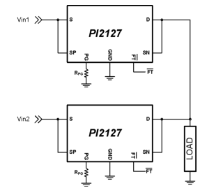
Typical Application:
Features
- Integrated High Performance 12A, 8.5mΩ MOSFET
- Very small, high density fully-optimized solution with simple PCB layout
- Fast dynamic response to power source failures, with 80ns reverse current turn-off delay time
- Accurate sensing capability to indicate system fault conditions (-6mV reverse threshold)
- Internal charge pump
- Active low fault flag output
Applications
- N+1 Redundant Power Systems
- Servers & High End Computing
- Telecom Systems
- High-side Active ORing
Package Information
The PI2127 is offered in the following package:
- 17-pin 7mm x 8mm thermally enhanced LGA package, achieving <10°C/W RθJ-PCB
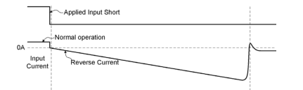
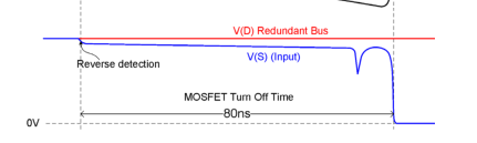
Figure 1: PI2127 High Side Active ORing
Figure 2: PI2127 response time to an input short fault condition
PI2127 Rev 1.3 Page 1 of 19
Page 2
Pin Description
| Pin Name | Pin Number | Description |
|---|---|---|
| NC | 1, 3, 5, 7 | Not Connected: Leave pins floating. |
| PG | 2 | Control Circuitry Return: This pin is the floating return path for the controller circuitry. Connect this pin via a resistor to the low side return (ground). |
| FT | 4 | Fault Status Output: This open collector pin pulls low to indicate one of the several potential fault conditions may exist. The Fault pin will pull low after a reverse or forward fault has been detected with a defined delay time (8μs). In addition, the FT pin will pull low when the controller input voltage is below the VC under-voltage threshold V < 7V S-PG (V ). When V > 7.15V (V ) and 6mV < V < 275mV this pin clears (High). SUVF S-PG SUVR SP-SN Leave this pin open if unused. |
| GND | 6 | FT Return: This pin is the return (ground) for the open collector fault circuitry. Connect this pin to logic ground. |
| SN | 8 | Negative Sense Input: Connect SN pin to the trace between D pin (outside of the PI2127 foot print) and the output load. The polarity of the voltage difference between SP and SN provides an indication of current flow direction through the MOSFET. |
| D | 9, 10, 11, 17 | Drain: The Drain of the internal N-channel MOSFET and fault level shift circuit. Connect this pin to the output load. |
| S | 12, 13, 14 16 | Source-The source of the internal N-channel MOSFET and bias for the control circuitry. Connect this pin to the input power source bus voltage. |
| SP | 15 | Positive Sense Input: Connect SP pin to the trace between S pin (outside of the PI2127 foot print) and the input source. The polarity of the voltage difference between SP and SN provides an indication of current flow direction through the MOSFET. |
Package Pin-Out
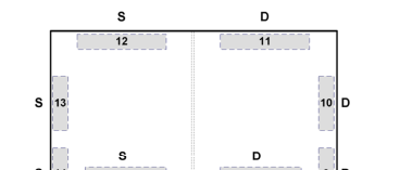
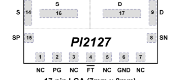
17-pin LGA (7mm x 8mm) Top view
PI2127 Rev 1.3 Page 2 of 19
Page 3
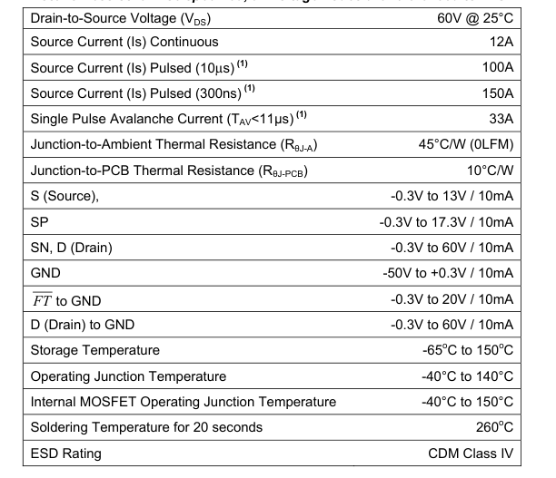
Absolute Maximum Ratings
Note: Unless otherwise specified, all voltage nodes are referenced to “PG”
Electrical Specifications
Unless otherwise specified: -40°C < TJ < 125°C, VS-PG =10.5V, VPG=VGND=0V, VD=VS
| Parameter | Symbol | Min | Typ | Max | Units | Conditions |
|---|---|---|---|---|---|---|
| Control Circuit Supply (S to PG) | ||||||
| Operating Supply Range | V S-PG | 8.5 | 10.5 | V | No VC limiting Resistor | |
| Quiescent Current | I VC | 1.5 | 2.0 | mA | Normal operation, no fault | |
| Clamp Voltage | V S-CLM | 11 | 11.7 | 12.5 | V | I =3mA S |
| Clamp Resistance | R S | 10 | Ω | Delta I =10mA S | ||
| Under-Voltage Rising Threshold | V SUVR | 6.1 | 7.15 | 8.5 | V | |
| Under-Voltage Falling Threshold | V SUVF | 6 | 7.00 | 7.9 | V | |
| Under-Voltage Hysteresis | V SUV-HS | 100 | 150 | 200 | mV | |
PI2127 Rev 1.3 Page 3 of 19
Page 4
Electrical Specifications
Unless otherwise specified: -40°C < TJ < 125°C, VS-PG =10.5V, VPG=VGND=0V, VD=VS
| Parameter | Symbol | Min | Typ | Max | Units | Conditions |
|---|---|---|---|---|---|---|
| DIFFERENTIAL AMPLIFIER AND COMPARATORS (Continued) | ||||||
| Common Mode Input Voltage | V CM | -3 | 3 | V | SP to S and SN to S | |
| Differential Operating Input Voltage(1) | V SP-SN | -80 | 400 | mV | SP-SN | |
| SP Input Bias Current | I SP | 35 | 55 | 75 | μA | V = V = V SP SN S |
| SN Input Bias Current | I SN | 35 | 55 | 75 | μA | V = V = V SP SN S |
| SN Current During Fault Condition(3) | I SN-FLT | 5 | 7.5 | mA | V = 60V, SN V = V =V =0V SP S D | |
| MOSFET Turn On Threshold | V FET-ON | +1 | +6 | +11 | mV | V = 10.5V, @ 25°C SP-PG |
| Reverse Comparator Threshold | V RVS-TH | -11 | -6 | -2 | mV | V = 10.5V, @ 25°C SP-PG |
| Reverse to On Hysteresis | V RVS-HY | 10 | 12 | 14 | mV | V = 10.5V, @ 25°C SP-PG |
| Reverse Fault to MOSFET Turn-off Time | t RVS | 80 | 150 | ns | V = ± 50mV step SP-SN | |
| Forward Comparator Threshold | V FWD-TH | 250 | 275 | 300 | mV | |
| Forward Comparator Hysteresis | V FWD-HY | 15 | 25 | 35 | mV | |
| Internal N-Channel MOSFET | ||||||
| Drain-to-Source Breakdown Voltage | BV DSS | 60 | V | V =V =V =V =0V S GND FT SP I =2mA , Tj=25°C; D V =10.5V SN | ||
| Source Current Continuous | I S | 12 | A | In ON state, Tj=25°C | ||
| D Pin Current During Fault (3) (including level-shift circuitry) | I D-FLT | 4 | mA | V =60V; D V =V =V =V =0V, GND FT S SP Tj=25°C, V =10.5V SN | ||
| Drain-to-Source On Resistance | R DSon | 8.5 | 11 | mΩ | In ON state, IS=10A, Tj=25°C | |
| Body Diode Forward Voltage | V F-BD | 0.75 | 1.0 | V | In OFF state, IS=4A, Tj=25°C | |
| Fault | ||||||
| Fault Output Low Voltage | V FT | 0.2 | 0.5 | V | I =2mA, V ≥ 4.5V FT S-PG | |
| Fault Output High, Leakage Current | I FT | 10 | μA | V =14V FT | ||
| Fault Delay time | T FT-DLY | 4 | 8 | 16 | μs | V = ± 50mV step SP-SN |
Note 1: These parameters are not production tested but are guaranteed by design, characterization, and correlation with statistical process control.
Note 2: Current sourced by a pin is reported with a negative sign.
Note 3: Current flow during input short fault condition. See the Fault Circuit description in the Application Information section for more detail
PI2127 Rev 1.3 Page 4 of 19
Page 5
Functional Description:
The PI2127 integrated Cool-ORing product takes advantage of two different technologies combining an 8.5mΩ on-state resistance (RDS(on)) N-channel MOSFET with high density control circuitry. This combination provides superior density, minimizing PCB space to achieve an ideal ORing diode function, significantly reducing power dissipation and eliminating the need for heat sinking, while minimizing design complexity.
The PI2127’s 8.5mΩ on-state resistance MOSFET used in the conduction path enables a dramatic reduction in power dissipation versus the performance of a diode used in conventional ORing applications due to its high forward voltage drop. Due to the inherent characteristics of the MOSFET, current will flow in the forward and reverse directions while the gate remains above the gate threshold voltage. Ideal ORing applications should not allow reverse current flow, so the controller has to be capable of very fast and accurate detection of reverse current caused by input power source failures, and very fast turn off of the gate of the MOSFET. Once the gate voltage falls below the gate
threshold, the MOSFET is off and the body diode will be reverse biased preventing reverse current flow and subsequent excessive voltage droop on the redundant bus.
Differential Amplifier: The PI2127 integrates a high-speed low offset voltage differential amplifier to sense the difference between the Sense Positive (SP) pin voltage and Sense Negative (SN) pin voltage with high sensitivity to fault current. The amplifier output is connected to the Reverse and Forward comparators.
Reverse Current Comparator: RVS The reverse current comparator provides the critical function in the controller, detecting negative voltage caused by reverse current. Gate drive is enabled when SP is 6mV higher than SN. When the SN pin is 6mV higher than the SP pin, the reverse comparator will force the gate discharge circuit to turn off the MOSFET in typically 80ns and assert the Fault ( FT ) low to report a fault condition.
The reverse comparator will hold the gate low until the SP pin is 6mV higher than the SN pin. The reverse comparator hysteresis is shown in Figure 3.
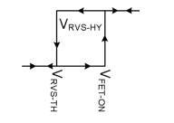
Figure 3: Reverse comparator hysteresis: VSP - VSN
Forward Voltage Comparator: FWD The FWD comparator detects when a forward voltage condition exists and SP is above 275mV (typical) positive with respect to SN. When SP-SN is more than 275mV, the FWD comparator will assert the Fault ( FT ) low to report a fault condition.
Internal Voltage Regulator: The PI2127 control circuitry and the gate driver are biased through the S pin. An internal regulator clamps the S voltage (VS-PG ) to 11.7V. The internal regulator circuit has a comparator to monitor S input with respect to the PG pin and pulls the MOSFET GATE low when VS-PG is lower than the Under- Voltage Threshold.
Fault Indication: FT The FT pin is an open collector NPN that will be pulled low during following fault conditions.
| Typical Condition | Indication of possible faults | ||
|---|---|---|---|
| 1 | Reverse: | V -V ≤ -6mV SP SN | Input supply shorted (MOSFET turned OFF) |
| 2 | Forward: | V -V ≥ +275mV SP SN | Open FET, Gate short, Gate open, or High current (MOSFET turned ON) |
| 3 | Forward | V -V ≤ +6mV SP SN | Shorted FET on power-up (MOSFET turned OFF) |
| 4 | UVLO | 4.5V < V <7.15V S-PG | Controller not ready (MOSFET turned OFF) |
PI2127 Rev 1.3 Page 5 of 19
Page 6
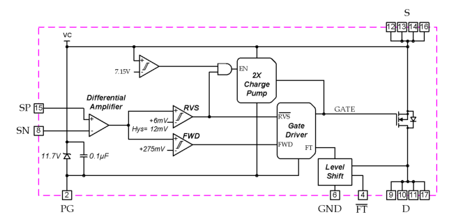
Figure 4: PI2127 Internal Block Diagram
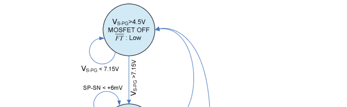
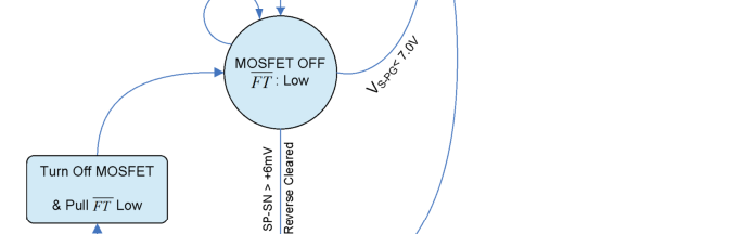
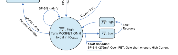
Figure 5: PI2127 State Diagram
PI2127 Rev 1.3 Page 6 of 19
Page 7
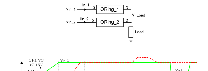
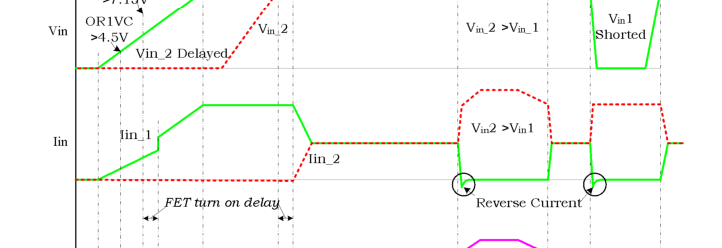
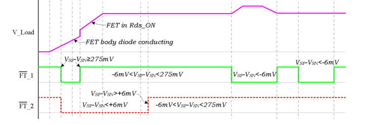
Figure 6: PI2127 Timing Diagram.
PI2127 Rev 1.3 Page 7 of 19
Page 8
Typical Characteristics:
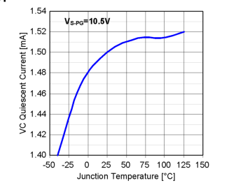
Figure 7: Controller bias current vs. temperature
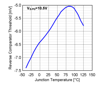
Figure 8: Reverse comparator threshold vs. temperature.
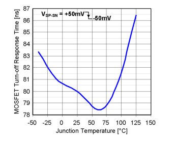
Figure 9: Reverse Fault to MOSFET Turn-off Response Time vs. temperature.
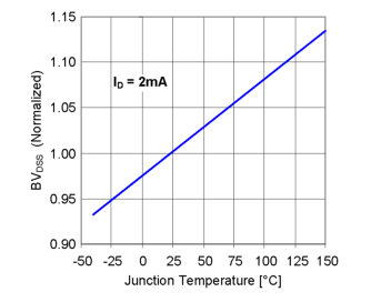
Figure 10: Internal MOSFET drain to source breakdown voltage vs. temperature.
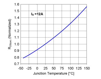
Figure 11: Internal MOSFET on-state resistance vs. temperature.
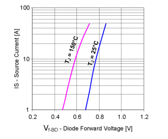
Figure 12: Internal MOSFET source to drain diode forward voltage (pulsed ≤300µs).
PI2127 Rev 1.3 Page 8 of 19
Page 9
Thermal Characteristics:
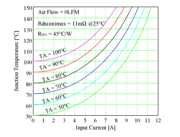
Figure 13: MOSEFT Junction Temperature vs. Input Current for a given ambient temperature (0LFM)
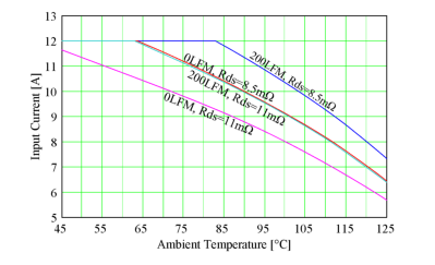
Figure 14: PI2127 input current de-rating based on the MOSFET maximum TJ=150°C vs. ambient temperature
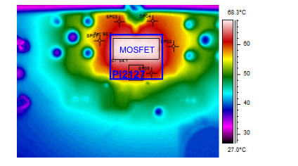
Figure 15: PI2127 mounted on PI2127- EVAL1Thermal Image picture, Iout=12A, TA=25°C, Air Flow=0LFM
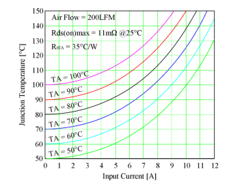
Figure 16: MOSFET Junction Temperature vs. Input Current for a given ambient temperature (200LFM)
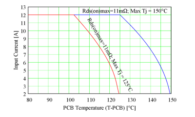
Figure 17: PI2127 input current de-rating vs. PCB temperature, for the MOSFET maximum TJ at 125°C and 150°C
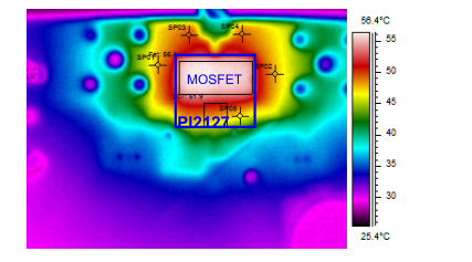
Figure 18: PI2127 mounted on PI2127-EVAL1 Thermal Image picture, Iout=10A, TA=25°C, Air Flow=200LFM
PI2127 Rev 1.3 Page 9 of 19
Page 10
Figure 19: Plot of PI2127 response time to reverse current detection
Application Information
The PI2127 is designed to replace high side ORing diodes in high current, medium voltage redundant power architectures. Replacing a traditional diode with a PI2127 will result in significant power dissipation reduction as well as board space reduction, efficiency improvement and additional protection features.
This section describes in detail the procedure to follow when designing with the PI2127 Active ORing solution.
Control Circuitry Bias: The PI2127 control circuitry and the gate driver for the internal MOSFET are biased through the S pin. An internal regulator clamps the S pin voltage (VS-PG) to 11.7V typically.
A bias resistor (RPG) is required if the voltage at the S pin is higher than the minimum Voltage Clamp (VS-
CLM). RPG should be connected between PG pin and ground (VS return).
Minimize the resistor value for low S voltage levels to avoid a voltage drop that may reduce VS-PG lower than required.
Select the value of RPG using the following equations:
− V V − −
RPG = S min S PGMax + I 1.0 mA VC max RPG maximum power dissipation:
− 2
V V (
)
S −max S −PGMin
Pd = RPG
RPG
Where: : S pin minimum applied voltage VS −min : S pin maximum applied voltage VS −max : Controller maximum clamp voltage, 12.5V V − S PGMax
PI2127 Rev 1.3 Page 10 of 19
Page 11
: Controller minimum clamp voltage, 11V V − S PGMin : Controller maximum bias current, use I VC max 2.0mA 1.0 mA : 0.1mA is added for margin
Example: 40V <VS-PG <50V
V −V
− V 125. V 40 −
=
=
= Ω
S min S PGMax
R
k 131.
PG
+ IC mA
mA
1.0
1.2
max
( )
−V
2
2 −
V (
) 50 V 11 V
− −
=
=
=
S max S PGMin
116mW
PdR PG
kΩ
R
131.
PG
Alternative Bias Circuit with Device Enable: Constant current circuit In a wide operating input voltage range the size of RPG may be become large to support power dissipation. A simple constant current circuit can be used instead of RPG to reduce power dissipation and can be used as a device enable.
As shown in Figure 20, the constant current circuit consists of an NPN transistor (Q1), Zener diode DZ, current limit resistor (RLIMIT) and Zener bias resistor (RZ). RLIMIT and RZ can be very low power resistors and Q1 is a signal transistor where its Collector- Emitter Voltage (VCEO) is equal or greater than the input operating voltage and supports 2.5mA at the operating input voltage.
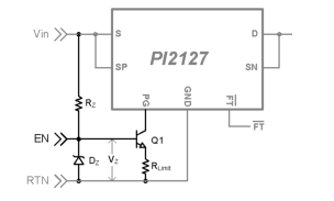
Figure 20: Constant current bias circuit
Pulling the Q1 base (EN) to the system return (RTN) will turn off the transistor and the controller return (PG pin) will float and eventually the MOSFET will be turned off. An open collector device can be used to enable and disable the PI2127.
The constant current circuit should guarantee current greater than the PI2127 maximum Quiescent current (IVC), 2.0mA.
RLIMIT can be calculated from the following equation:
− V (on) V Z _ MIN BE
= R LIMIT
I VC _ MAX
Where: VZ _ MIN : Minimum Zener diode voltage
VBE (on) : Q1 Base-Emitter On maximum voltage, for default use (on) =0.7V
VBE
Zener Diode Selection: Select a Zener diode with a low reverse current requirement to minimize RZ. Zener diodes with higher break down voltage will have lower reverse current and reduce Q1 collector current variation. Zener diodes with a breakdown voltage of 6V and higher will require low bias current for accurate voltage breakdown.
RZ maximum value can be calculated with the following equation:
Note that the surface mount resistors have limited operating voltage capability. Be sure to pick a resistor package that can meet the maximum operating voltage (Vin).
− V V in _ MIN Z _ MAX
R = Z + I I B _ MAX Z Where:
Vin _ MIN
: Min input voltage
V _ : Zener diode maximum breakdown voltage Z MAX ZI : Zener diode required reverse current
BI _ MAX
: Q1 required maximum base current which calculated from the following equation:
I C _ MAX
= I B _ MAX
hFE _ MIN
I : Q1 maximum expected collector current. C _ MAX h : Q1 minimum gain. FE _ MIN
Internal N-Channel MOSFET BVDSS: The PI2127’s internal N-Channel MOSFET breakdown voltage (BVDSS) is rated for 60V at 25°C and will degrade to 55.5V at -40°C, refer to Figure 10. Drain to source voltage should not exceed BVDSS in nominal operation. During a fast switching transient the MOSFET can tolerate voltages higher than its BVDSS rating under avalanche conditions, refer to the Absolute Maximum Ratings table.
In Active ORing applications when one of the input power sources is shorted, a large reverse current is
PI2127 Rev 1.3 Page 11 of 19
Page 12
sourced from the load through the MOSFET. Depending on the output impedance of the system and the parasitic inductance, the reverse current in the MOSFET may exceed the source pulsed current rating (150A) just before the PI2127 MOSFET is turned off.
The peak current during an input short condition is calculated as follows, assuming that the output has very low impedance and it is not a limiting factor:
V \*t = S RVS
I PEAK
LPARASITIC
Where:
I : Peak current in PI2127 MOSFET before it is
PEAK turned off. V : Input voltage or load voltage at S pin before S input short condition did occur.
t : Reverse fault to MOSFET turn-off time.
RVS L :Circuit parasitic inductance PARASITIC
The high peak current during an input short and before the MOSFET turns off, stores energy in the circuit parasitic inductance, and as soon as the MOSFET turns off, the stored energy will be released and this will produce a high negative voltage and ringing at the MOSFET source. At the same time the energy stored at the drain side of the internal MOSFET will be released and produce a voltage higher than the load voltage. This event will create a high voltage difference between the drain and source of the MOSFET. The MOSFET will avalanche, but this avalanche will not affect the MOSFET performance because the PI2127 has a fast response time to the input fault condition and the
stored energy will be well below the MOSFET avalanche capability.
MOSFET avalanche during input short is calculated as follows:
3.1 \* BV 1
2
=
DSS \* L \* I
E \*
PARASITIC PEAK
AS
−
2 3.1 \* BV
V DSS S
Where: E AS : Avalanche energy
BVDSS
: MOSFET breakdown voltage (60V)
Power dissipation: In Active ORing circuits the MOSFET is always on in steady state operation and the power dissipation is derived from the total source current and the on-state resistance of the MOSFET.
The PI2127 internal MOSFET power dissipation can be calculated with the following equation:
= ∗ 2
Pd
Is R MOSFET
DS (on)
Where: Is: Source Current : MOSFET power dissipation Pd MOSFET RDS(on): MOSFET on-state resistance
Note: For the worst case condition, calculate with maximum rated RDS(on) at the MOSFET maximum operating junction temperature because RDS(on) is temperature dependent. Refer to Figure 11 for normalized RDS(on) values over temperature. The PI2127 maximum RDS(on) at 25°C is 11mΩ and will increase by 43% at 125°C junction temperature.
The Junction Temperature rise is a function of power dissipation and thermal resistance.
= ∗
= ∗ ∗ 2
Trise R Pd
R Is R
θ
θ
JA MOSFET JA DS(on)
Where: Rθ : Junction-to-Ambient thermal resistance JA (45°C/Watt)
This may require iteration to get to the final junction temperature. Figure 13 and Figure 16 show the PI2127 internal MOSFET final junction temperature curves versus conducted current at maximum RDS(on), given ambient temperatures and air flow.
Fault Circuit: FT is an open collector pin and should be pulled up to the logic voltage via a resistor (10KΩ). An internal level shift circuit is implemented to change the PI2127 controller fault output reference from the PG pin voltage level to the GND pin voltage level. The level shift circuit is biased from the D pin to stay active when the bias voltage at S pin is not available. In the event of an input short fault condition, the S pin will be pulled low (ground) and the PI2127 control circuit will lose its bias voltage. If the output voltage is supplied from a redundant source, then the level shifter stays biased and the FT pin will be pulled low to indicate that the MOSFET is in the OFF condition.
During start-up and before the output voltage is established, the FT pin will be floating until the approximately 4.5V is present at the S pin or at D pin. Thereafter the FT pin is pulled low and stays low until the PI2127 controller bias voltage VS-PG increases above the controller Under-Voltage Threshold (VSUVR) and no fault conditions are present. Once this
PI2127 Rev 1.3 Page 12 of 19
Page 13
happens, the MOSFET is turned on and the FT pin will be high resistance to indicate that the MOSFET is in RDS(on) with no fault conditions existing.
Note that in case of an input fault condition, where the S pin is at ground and the output (D pin and SN pin) are at a high voltage there will be two current paths, one path from D pin to GND and the other path from SN pin to SP.
The current path from D pin to GND and S pins is due to the level shift circuit and will draw current from the output as a function of the voltage between D pin and GND (VD-GND) based on the following equation:
− 5.0 V
V D−GND = I − D FLT
15kΩ
Where: : Maximum D pin current during input short I − D FLT fault condition : Voltage difference between the D pin and VD−GND ground.
The current path from SN pin to S pin is a function of the SN voltage based on the following equation:
SN GND − V 12 V − = I SN _ FLT
RPAR
Where: : SN current during input short fault condition I SN _ FLT : Voltage difference between SN pin (or load VSN GND − voltage) and ground. R : Resistance of the internal path, 10KΩ PAR typical and 8kΩ minimum
The level shift circuit worst case power dissipation during input short is:
− 2
V
V )
( 5.0 D−GND Pd = 15kΩ
The thermal resistance and power dissipation of the level shift circuit will limit the voltage applied at the D pin during a shorted input condition. When the PCB temperature exceeds 110°C, the applied voltage must be derated according to Figure 21. The plot in Figure 21 is calculated using the worst case power dissipation during an input short with RθJ-PCB= 100°C/W.
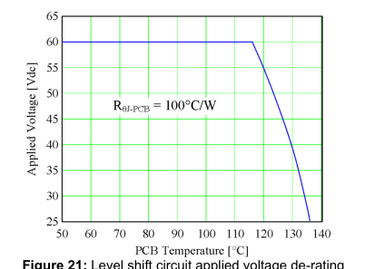
(valid during an input short fault condition as a function of PCB Temperature)
PI2127 Rev 1.3 Page 13 of 19
Page 14
Typical Application Example:
Requirement: Redundant Bus Voltage = 40V ±5V Maximum Load Current = 9A (assume through each redundant path) Maximum Ambient Temperature = 60°C, no air flow (0LFM) The current flow parasitic inductance for each ORing device is 60nH.
Solution: A single PI2127 for each redundant 40V power source should be used, configured as shown in the circuit schematic in Figure 23.
RPG selection:
35V <VS-PG <45V
−
−
V V 35 V 125. V
S −PGMax =
=
= Ω
S min R
10.71 k
PG IC + 1.0 mA 1.2 mA
max
The closest 1% resistor available is 10.5kΩ
( )
−
2
2 −
V V (
) 45 V 11 V
− −
=
PG =
=
S max S PGMin
PdR
110mW
105.kΩ
R PG
The selected resistor should be capable of supporting the total power at maximum operating temperature, 60°C. An 0805 (2012) will support the power requirement.
FT pin: Connect FT pin to the logic input and to the logic power supply via a resistor, as required for the proper input level of the supervisor functions.
Power Dissipation and Junction Temperature: First use Figure 13 (Junction Temperature vs. Input Current) to find the final junction temperature for 9A load current at 60°C ambient temperature. In Figure 13 (illustrated in Figure 22) draw a vertical line from 9A to intersect the 60°C ambient temperature line. At the intersection draw a horizontal line towards the Y- axis (Junction Temperature). The Junction Temperature at maximum load current (9A) and 60°C ambient is 115°C.
RDS(on) is 11mΩ maximum at 25°C and will increase as the Junction temperature increases. From Figure 11, at 115°C RDS(on) will increase by 38%, then
= Ω∗ =
Ω maximum at 115°C
R 11 m .138 15
.18 m
DS(on) Maximum power dissipation is:
= ∗
= ∗ Ω =
2
2
Pd Iin R
9(A ) 15 .18 m .123 W
DS(on)
max
Recalculate TJ:
° ⎛ 45
⎞
C
= 60 ° C +⎜ ∗9(A ) ∗15 Ω⎟ =115 °
2 .18 m 3. C
TJ max
W ⎝
⎠
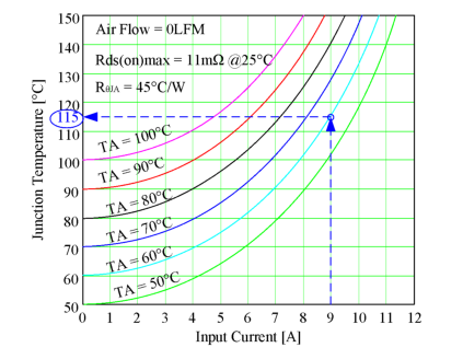
Figure 22: Example 1 final MOSFET junction temperature at 9A/60°C TA
Reverse Current Threshold: The following procedure demonstrates how to calculate the minimum required reverse current in the internal MOSFET to generate a reverse fault condition and turn off the internal MOSFET.
At maximum junction temperature (115°C) and maximum RDS(on):
RVS TH − V
6mV − = =
= −
Is.reverse
395mA
15.18mΩ R DS (on)
Peak current under input short is:
At typical response time:
V \* t
45 V \* 80ns
=
=
=
S RVS
I
60A
PEAK L
60nH
PARASITIC
PI2127 Rev 1.3 Page 14 of 19
Page 15
At maximum response time:
V \* t
45 V \*150ns
=
=
=
S RVS
I
1125.A
PEAK L
60nH
PARASITIC
Avalanche Energy:
1 3.1 \* BV
2
=
DSS
E \*
\* L \* I
AS
PARASITIC PEAK
2 3.1 \* BV − V
DSS S
3.1\*60 1
2 = μ
= E AS
\*60nH \*1125.A 897 J
\* −
2 3.1\*60 V 45 V
The avalanche energy is well below the total MOSFET specified peak current of 150A for 300ns and below the rated avalanche energy. The specified energy can be calculated from Single Pulse Avalanche Current as specified in the Absolute Maximum Ratings table:
1
1
⋅
⋅ ⋅ =
⋅ ⋅ ⋅ μ =
3.1\* BV I t
3.1 60 V 33A 11 s 14mJ
DSS AS AV
2
2
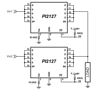
Figure 23 : Two PI2127 in High Side ORing configuration
VC bias through Constant current circuit Select an NPN transistor with VCEO equal or higher than the input voltage (Vin) plus any expected transient voltage and capable of handling the expected maximum power dissipation. Any NPN transistor with VCEO ≥ 60V in a small footprint is suitable. An exemplary NPN is the BC846 from NXP Semiconductors:
From the BC846 datasheet: NPN general-purpose transistor VCEO = 65V Collector-Emitter maximum voltage IC = 100mA maximum collector current hFE = 110 minimum at IC=2mA VBE = 0.580V to 0.70V Base-Emitter voltage at IC = 2mA and 25°C RθJ-A = 500°C/W Junction to ambient thermal resistance.
Select Zener Diode: A Zener diode with low bias current and VZ=10 in small foot print is suitable for this application. An exemplary Zener diode is the MM3Z10VST1 the from ON Semiconductor
From the MM3Z10VST1 datasheet: 10V, 200mW Zener Diode VZ = 9.80V to 10.2V Zener voltage range IR = 10μA will hold the Zener breakdown voltage at 9.8V
−V (on) V
V − 7.0 8.9 V
Z _ MIN BE
=
=
= Ω
R
.433k
LIMIT
I
1.2 mA
VC _ MAX
Or 4.32kΩ 1%
I C _ MAX 3mA
= 27.27μ
= =
I
A
B _ MAX h 110 FE _ MIN
RZ Calculation:
Use 120μA as minimum for the Zener diode reverse leakage current and Q2 base current combined.
− V V
−
Z _ MAX 40 V 102. V
in _ MIN Z =
=
= Ω
R
248k μ
+ I I
120 A
Z B _ MAX
Select RZ= 249kΩ 1%
Maximum Q1 collector current:
− V V
V − .050
BE _ MIN 102.
V
Z _ MAX =
=
=
I
.229mA
C _ MAX
Ω
R
.432k \* .098
LIMIT _ MIN
Maximum Q2 power dissipation
=
− − −
Pd I
\*[ Vin V ( V V )]
VC−CLM
Q1 C _ MAX
Z _ MIN EB _ MAX
MAX
PdQ1 =
− −
− =
.229mA\*[45
V 11 V (8.9 V 7.0 V )] 57mW
Transistor temperature rise
° C
=
=
= °
Pd \*R
mW \*
. C
T
θ −
RISEQ Q J A
W
PI2127 Rev 1.3 Page 15 of 19
Page 16
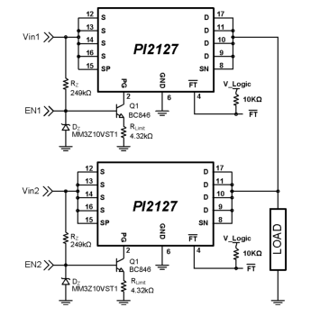
Figure 24: PI2127 in high side +48V application, VC is biased through constant current circuit.
Layout Recommendation:
Use the following general guidelines when designing printed circuit boards. An example of the typical land pattern for the PI2127 is shown in Figure 25:
- Make sure to have a solid ground (return) plane to reduce circuit parasitic.
- Connect all S pads together with a wide trace to reduce trace parasitics to accommodate the high current input, and also connect all D pads together with a wide trace to accommodate the high current output.
- Connect the SP pin to the S pins and connect the SN pin to D pins as shown in Figure 25.
- Use 1oz of copper or thicker if possible to reduce trace resistance and reduce power dissipation.
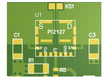
Figure 25: PI2127 layout recommendation
PI2127 Rev 1.3 Page 16 of 19
Page 17
Package Drawing:
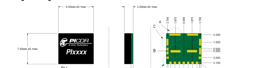
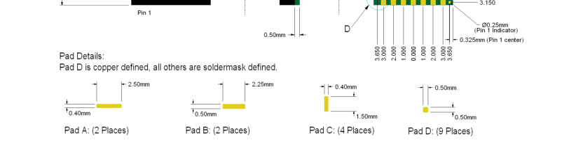
Ordering Information
| Part Number | Package | Transport Media |
|---|---|---|
| PI2127-01-LGIZ | 7mm x 8mm 17-pin LGA | T&R |
PI2127 Rev 1.3 Page 17 of 19
Page 18
Footprint Recommendation:
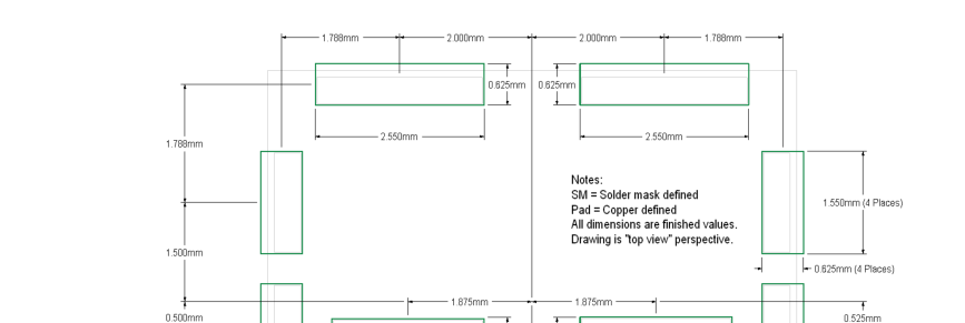
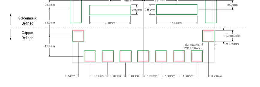
PI2127 Rev 1.3 Page 18 of 19
Page 19
Warranty
Vicor products are guaranteed for two years from date of shipment against defects in material or workmanship when in normal use and service. This warranty does not extend to products subjected to misuse, accident, or improper application or maintenance. Vicor shall not be liable for collateral or consequential damage. This warranty is extended to the original purchaser only.
EXCEPT FOR THE FOREGOING EXPRESS WARRANTY, VICOR MAKES NO WARRANTY, EXPRESS OR LIMITED, INCLUDING, BUT NOT LIMITED TO, THE WARRANTY OF MERCHANTABILITY OR FITNESS FOR A PARTICULAR PURPOSE.
Vicor will repair or replace defective products in accordance with its own best judgment. For service under this warranty, the buyer must contact Vicor to obtain a Return Material Authorization (RMA) number and shipping instructions. Products returned without prior authorization will be returned to the buyer. The buyer will pay all charges incurred in returning the product to the factory. Vicor will pay all reshipment charges if the product was defective within the terms of this warranty.
Information published by Vicor has been carefully checked and is believed to be accurate; however, no responsibility is assumed for inaccuracies. Vicor reserves the right to make changes to any products without further notice to improve reliability, function, or design. Vicor does not assume any liability arising out of the application or use of any product or circuit; neither does it convey any license under its patent rights nor the rights of others. Vicor general policy does not recommend the use of its components in life support applications wherein a failure or malfunction may directly threaten life or injury. Per Vicor Terms and Conditions of Sale, the user of Vicor components in life
support applications assumes all risks of such use and indemnifies Vicor against all damages.
Vicor’s comprehensive line of power solutions includes high density AC-DC and DC-DC modules and accessory components, fully configurable AC-DC and DC-DC power supplies, and complete custom power systems.
Information furnished by Vicor is believed to be accurate and reliable. However, no responsibility is assumed by Vicor for its use. Vicor components are not designed to be used in applications, such as life support systems, wherein a failure or malfunction could result in injury or death. All sales are subject to Vicor’s Terms and Conditions of Sale, which are available upon request.
Specifications are subject to change without notice.
Vicor Corporation 25 Frontage Road Andover, MA 01810 USA
Picor Corporation 51 Industrial Drive North Smithfield, RI 02896 USA
Customer Service: custserv@vicorpower.com Technical Support: apps@vicorpower.com
Tel: 800-735-6200 Fax: 978-475-6715
PI2127 Rev 1.3 Page 19 of 19