


 Download PDF
DATASHEET SEARCH SITE
Document overview
- PDF pages: 16
Technical content
Page 1
Cool-Switch® Series
High Side High Voltage Load Disconnect Switch Controller IC
Description
The PI2061 is a high-speed electronic circuit breaker controller IC designed for use with N-channel MOSFETs in high side load disconnect switch solutions for medium voltage applications. The PI2061 Cool-Switch® controller enables an extremely low power loss solution with fast dynamic response to an over current fault or EN Low conditions.
Once enabled, the PI2061 monitors the MOSFET current through a sense resistor. If an over current level is sensed, the switch is quickly latched off to prevent the power source from being overloaded. Bringing the EN pin low will reset the over current latch allowing retry. To avoid false tripping by the in-rush current, the over current level is approximately doubled during start up, until SN approaches about 0.8V below VC. The PI2061 has an internal charge pump to drive the gate of a high side N-Channel MOSFET above the VC input. There is an internal shunt regulator that regulates the VC input with respect to the SGND pin for applications higher than 11
volts.
Features
Programmable latching over-current detection Fast 120ns disconnect response to a load short Fast disable via EN pin, typically 200ns. 4A gate discharge current Internal charge pump Fault status indication
Applications
Telecom System, ≤80V operation & 100V/100ms Transient N+1 Redundant Power Systems Servers & High End Computing High Side Circuit Breaker and Load Disconnect
Package Information
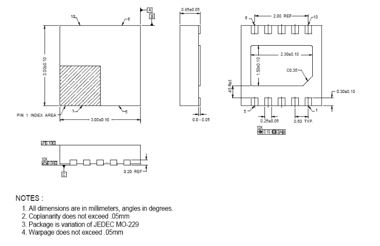
The PI2061 is offered in the following package: 10 Lead 3mm x 3mm DFN package
Typical Application:
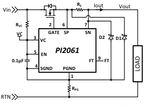
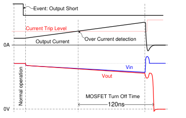
Figure 1: PI2061 in High Side Disconnect switch application Figure 2: PI2061 response time to output short fault condition
Page 1 of 16
Page 2
Pin Description
| Pin Name | Pin Number | Description |
|---|---|---|
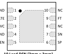
| PGND | 1 | Gate Driver Switch Return: This pin is the high current return path for the gate driver turn off switch. Connect this pin to the low side of VC bypass capacitor and SGND. |
| GATE | 2 | Gate Drive Output: This pin drives the gate of the external N-channel MOSFET. Under normal operating conditions, the GATE pin pulls high to approximately 2*VC with respect to SGND pin. The controller turns the GATE off during an over-current fault that is above the overcurrent voltage threshold (166mV during power up and 70mV in steady state). |
| VC | 3 | Controller Input Supply: This pin is the supply pin for the control circuitry and gate driver. Connect a 0.1μF capacitor between the VC pin and the SGND pin. Voltage on this pin is regulated to 11.7V with respect to SGND by an internal shunt regulator. Connect a bias resistor (R ) between the VC VC pin and the supply input as shown in Figure 1. |
| SGND | 4 | VC Return: This pin is the return (ground) for the control circuitry. Connect this pin to the low side of the VC bypass capacitor and high side of the R resistor as shown in Figure 1. PG |
| EN | 5 | Enable: Pull this pin low with 8µA or more to disable the gate driver and reset the latch. Tie this pin to VC if the Enable/disable feature is not used. |
| SP | 6 | Positive Sense Input & Clamp: Connect SP pin to the positive side of the sense resistor. The magnitude of the voltage difference between SP and SN provides an indication of the current through the sense resistor. |
| SN | 7 | Negative Sense Input & Clamp: Connect SN pin to the negative side of the sense resistor. The magnitude of the voltage difference between SP and SN provides an indication of the load current through the sense resistor. |
| NC | 8, 10 | No Connect: Leave pins unconnected |
| FT | 9 | Fault Status Output: This open collector pin transitions to high resistance to indicate a fault. When the controller input voltage is in under voltage, VC - SGND < 7V this pin is high resistance as well. When the part is in a normal operating condition and gate driver is enabled this pin is low resistance. |
Package Pin-Outs
PGND
GATE
SGND
10 Lead DFN (3mm x 3mm) Top view
Page 2 of 16
Page 3
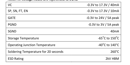
Absolute Maximum Ratings
Note: All voltage nodes are referenced to SGND
Electrical Specifications
Unless otherwise specified: -40C < TJ < 125C, VC=EN=10.5V, CVc =0.1uF, CGATE_PGND =1nF, SGND=PGND
| Parameter | Symbol | Min | Typ | Max | Units | Conditions | |
|---|---|---|---|---|---|---|---|
| VC Supply | |||||||
| Operating Supply Range | V VC-SGND | 8.5 | 10.5 | V | No VC limiting Resistor | ||
| Quiescent Current | I VC | 1.7 | 2.1 | mA | VC = 10.5V, SP=SN=VC | ||
| Quiescent Current Start Up | I VCSU | 2.0 | 2.5 | 3.0 | mA | VC = 8.5V, SP=SN=SGND | |
| VC Clamp Voltage | V VC-CLM | 11 | 11.7 | 12.5 | V | I =3mA VC | |
| VC Clamp Series Resistance | R VC | 10 | | Delta I =10mA VC | |||
| VC Under-Voltage Rising Threshold | V VCUVR | 6.2 | 7.32 | 8.5 | V | ||
| VC Under-Voltage Falling Threshold | V VCUVF | 6 | 7.00 | 7.9 | V | ||
| VC Under-Voltage Hysteresis | V VCUV-HS | 240 | 320 | 400 | mV | ||
| DIFFERENTIAL AMPLIFIER AND COMPARATORS | |||||||
| Common Mode Input Voltage | V CM | V SGND | V +0.3 VC | V | |||
| Differential Operating Input Voltage(1) | V SP-SN | 250 | mV | SP-SN | |||
| SP Input Bias Current | I SP | 15 | 25 | 35 | μA | SP=SN=VC | |
| SN Input Bias Current | I SN | 25 | 37 | 50 | μA | SP=SN=VC | |
| D Forward Voltage BST | V DBST | 0.87 | 1.0 | V | I =3mA SN | ||
| Low Range Overcurrent Threshold | V OC-THL | 63 | 70 | 77 | mV | VC-SN=0V | |
| Low Range Overcurrent Turn-off Time | T OC-OFF | 120 | 200 | ns | V = 0V to 200mV step to 90% SP-SN of VG max, SN=VC | ||
| High Range Overcurrent Threshold | V OC-THH | 133 | 166 | 200 | mV | VC-SN=6V | |
| Overcurrent Hysteresis(1) | V OC-HY | 9 | 13 | 17 | mV | ||
Page 3 of 16
Page 4
Electrical Specifications
Unless otherwise specified: -40C < TJ < 125C, VC=EN=10.5V, CVc =0.1uF, CGATE_PGND =1nF, SGND=PGND
| Parameter | Symbol | Min | Typ | Max | Units | Conditions |
|---|---|---|---|---|---|---|
| DIFFERENTIAL AMPLIFIER AND COMPARATORS (continued) | ||||||
| Over Current Range switch over Threshold | V SOTH | 0.5 | 0.8 | 1 | V | VC-SN |
| Over Current Range switch over delay(1): Low to high threshold | T SOL2H | 100 | 170 | 300 | ns | VC-SN= -0.7V~1.7V |
| Over Current Range switch over delay(1): High to low threshold | T SOH2L | 80 | 125 | 190 | ns | SN-VC= -1.7V~0.7V |
| GATE DRIVER | ||||||
| Gate Source Current | I G-SC | -15 | -10 | µA | V =V -1, I =3mA G G-Hi VC | |
| Pull Down Peak Current to PGND(1) | I G-PD | 1.5 | 4.0 | A | ||
| Pull-down Gate Resistance to PGND(1) | R G-PD | 0.3 | | V = 1.5V @ 25C G | ||
| AC Gate Pull-down Voltage to PGND(1) | V G-PGND | 0.2 | V | |||
| DC Gate Pull-down Voltage | V G-SGND | 0.8 | 1.2 | V | I =100mA, in OC Fault G | |
| Gate Drive Voltage to VC | V G-Hi | 7.0 | 8.0 | 11 | V | I =10μA, I =3mA G VC |
| 8.0 | 9.0 | 11 | V | I =2μA, I =3mA G VC | ||
| Gate Fall Time | t G-F | 10 | 25 | ns | 90% to 10% of V max. G | |
| Gate Voltage @ VC=4.5V | V G-UVLO | 0.7 | 1 | V | I =10µA, SP= SN=open G | |
| Enable (EN) | ||||||
| EN Threshold Voltage to VC pin | V VC_EN | 0.70 | 1.35 | 1.80 | V | |
| Disable pull down current | I dis | 8 | 15 | 22 | µA | |
| Fault Status: FT | ||||||
| FT Output Low Voltage | V FT | 0.2 | 0.5 | V | I =200µA, VC>8.5V FT | |
| FT Output High Leakage Current | I FT | 10 | μA | V =14V FT | ||
| FT Delay time | T FT-DLY | 2.5 | 5.5 | 12 | µs | V = 0~200mV step to 10% of SP-SN V max, SN=VC FT |
Note 1: These parameters are not production tested but are guaranteed by design, characterization, and correlation with statistical process control.
Note 2: Current sourced by a pin is reported with a negative sign.
Page 4 of 16
Page 5
Functional Description:
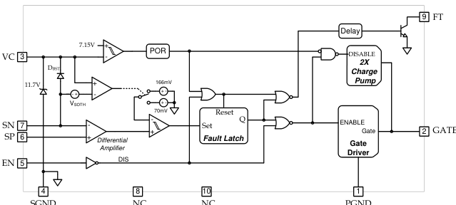
The PI2061 Cool-Switch is designed to drive an N-channel MOSFET in a high side Circuit Breaker application. As shown in Figure 1, the load current is sensed through the sense resistor (Rs). At power up the controller has a higher threshold voltage compared to steady state operation to allow capacitive load charging without nuisance tripping of the breaker.
Differential Amplifier: The PI2061 integrates a high-speed fixed offset voltage differential amplifier to sense the difference between the Sense Positive (SP) pin and Sense Negative (SN) pin voltage with high accuracy. The amplifier output is connected to the control logic that determines the state of the fault latch. To avoid tripping the breaker due to load capacitance during initial power up a higher threshold is used. The amplifier will detect if the drop across the sense resistor reaches 166mV and discharge the gate of the MOSFET if detected. Once the load voltage approaches the input potential the threshold is lowered to 70mV. This allows for capacitive load
charging and continuous current sensing without the use of a fixed sense blanking timer where excessive currents may develop glitching the input bus prior to breaking.
VC Voltage Regulator and MOSFET Drive: The biasing scheme in the PI2061 uniquely enables the gate control relative to SGND and PGND pins via the resistor RPG shown in Figure 1. The VC input provides power to the control circuitry, the charge pump and the gate driver. An internal regulator clamps the VC voltage to 11.7V with respect to SGND.
The VC pin is connected through an external resistor to the input power source and drain of the MOSFET. VC switches over to the load potential once the gate drive is enabled and over current condition is not present.
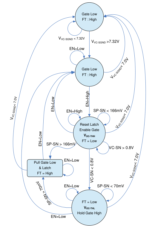
The internal regulator circuit has a comparator to monitor VC voltage and pulls the gate low when VC to SGND is lower than the VC Under-Voltage Threshold. As shown in Figure 1 the lower bias resistor, RPG is placed between the SGND connection and the system ground.
Gate Driver: The PI2061 has an integrated charge pump that approximately doubles the regulated VC with respect to SGND enhancing the N-Channel MOSFET gate to source voltage.
The internal gate driver controls the N-channel MOSFET such that in the on state, the gate driver applies current to the MOSFET gate driving it to bring the load up to the input voltage and into the RDS(on) condition.
When an over current condition is sensed the gate driver pulls the gate low to PGND and discharges the MOSFET gate with 4A peak capability. A Schottky diode (D1 in Figure 1) from PGND to the MOSFET source is required to direct the Gate high discharge current into the Source.
The PI2061 applies high gate discharge current for fast MOSFET turn off when a fault condition occurs to prevent system disruption. Fast MOSFET turn off may produce high voltage ringing due to parasitic inductance. To prevent negative peaks at SN from injecting substrate current, Schottky diode D2 (from SGND/PGND to SN pin as shown in Figure 1) is required.
Enable Input: (EN) This input provides control of the switch state enabling and disabling with low current level signals. The active high feature allows pulling/sinking a low current from this input to disable the breaker. System control can disable the switch and reset the over current latch by pulling this pin to a logic low state.
Once enabled, the Gate pin will charge the MOSFET gate to turn the load on. The load voltage will rise, reach the input voltage and the device will sense the current continuously once the POR interval has cleared relative to the VC to SGND potential. The disable control with this input is very fast, turning the switch off in typically 200ns. The response to open during an over current event is typically 120ns and the switch will latch off until reset by bringing this input low or recycling of the input power.
Fault Status: (FT) This open collector pin transitions to high resistance after the Fault Status is delayed for 5μs when an over-current fault or disable signal occurs. When the controller input voltage is in under voltage, (VC - SGND < 7V) this pin is high resistance as well. When the part is in a normal operating condition and gate driver is enabled this pin is low resistance. In high voltage applications this output must be translated to the system return with external circuitry. Leave this pin open if unused.
Page 5 of 16
Page 6
SGND
NC
PGND
NC
Figure 3: PI2061 Block Diagram
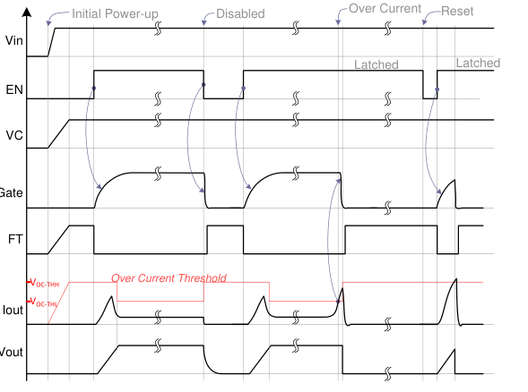
Figure 4: PI2061 Timing Diagram, referenced to Figure 1.
Page 6 of 16
Page 7
.
Figure 5: PI2061 State Diagram
Page 7 of 16
Page 8
Typical Characteristics:
1.72
1.70
1.68
1.66
1.64
1.62
1.60
1.58
-50 -25 0 25 50 75 100 125 150 Junction Temperature [°C]
Figure 6: Controller quiescent current vs. temperature.
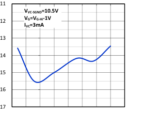
-50 -25 0 25 50 75 100 125 150 Junction Temperature [°C]
Figure 8: Gate source current vs. temperature
132
130
128
126
124
122
120
118
-50 -25 0 25 50 75 100 125 150 Junction Temperature [°C]
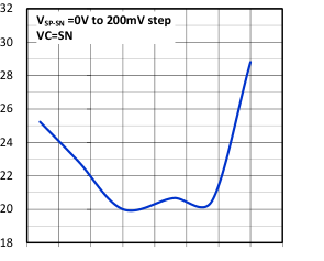
Figure 10: Low Range Overcurrent Turn-off time vs.
temperature.
7.36
7.34
7.32
7.30
7.28
7.26
7.24
-50 -25 0 25 50 75 100 125 150 Junction Temperature [°C]
Figure 7: VC Under-Voltage Rising threshold vs.
temperature
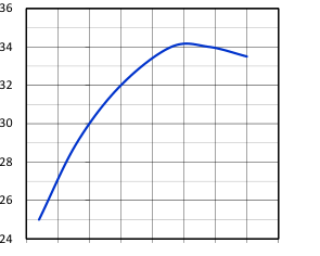
-50 -25 0 25 50 75 100 125 150 Junction Temperature [°C]
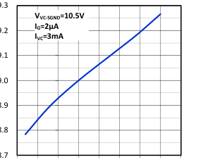
Figure 9: Gate drive voltage to VC vs. temperature.
71.0
70.5
70.0
69.5
69.0
68.5
68.0
-50 -25 0 25 50 75 100 125 150 Junction Temperature [°C]
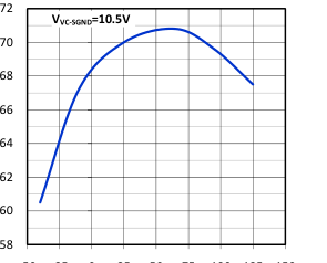
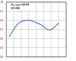
Figure 11: Low Range Overcurrent Threshold vs.
temperature.
Page 8 of 16
Page 9
Application Information
The PI2061 Cool-Switch is a wide input voltage high side load disconnect switch.
This section describes in detail the procedure to follow when designing with the PI2061 load disconnect switch.
Biasing sequence Functionality When Vin is applied and the load is at zero volts, the VC capacitor will charge via current flowing through RVC, D1, load resistance and RPG. If the load resistance is much lower than RPG, most of the charge and bias current flows through the load.
As VC to SGND voltage rises above the Under-Voltage Rising Threshold (VVCUVR) while the EN pin is High, the controller will charge the MOSFET gate and monitor the voltage across the sense resistor (VSP-SN). As the MOSFET turns on, the load voltage (Vout) will rise until the MOSFET is in RDS(on) and Vload=Vin. If the voltage across the sense resistor ( ) is higher than the High Range Overcurrent Threshold (VOC-THH 166mV) while the load rises, the gate will be discharged to PGND and latch off; otherwise Vout will keep rising, D1 becomes reverse biased and the controller bias current returns to ground through RPG.
When Vout reaches the Over Current Range switch over threshold, the over current threshold switches to the Low Range Over Current threshold (VOC-THL 70mV). VC will be biased from Vout through the SN pin when Vout is a diode drop (DBST) above VC as the load reaches Vin.
Upper and lower bias resistors should be selected to keep PI2061 bias voltage in regulation.
Upper Side Bias Resistor selection: RVC RVC is placed between Vin and VC to limit the current into the clamp under a shorted load condition. This will allow VC to regulate with respect to SGND/PDND node when the MOSFET is in off condition and SGND/PGND node is pulled low via D1, Rs and low load resistance.
The RVC resistor can be calculated using the following expression:
And RVC maximum power dissipation is:
Where: : Vin minimum voltage (Vin to Rtn) : Vin maximum voltage (Vin to Rtn) : VC maximum clamp voltage, 12.5V : VC minimum clamp voltage, 11V : VC maximum quiescent current at startup, use 3.0mA : D1 voltage drop, use 0.3V : 0.1mA is added for margin
Lower Side Bias Resistor selection: RPG RPG is placed between SGND/PGND and return to limit the clamp current and allow VC regulation when the MOSFET is in the on condition.
The RPG resistor can be calculated using the following expression:
And RVC maximum power dissipation is:
Where: : Boot Strap diode minimum forward voltage, use 0.8V : Boot Strap diode minimum forward voltage, use 1.0V : VC maximum quiescent current, use 2.1mA
RVC and RPG calculation example Vin (minimum) = 40V and Vin (maximum) = 50V
Note that in the case of a light load while the PI2061 is disabled, a voltage will appear at Vout due to the resistance between the VC pin and the SP and SN pins. The approximate value will be:
Where:
: Output load resistance when the load is inactive
Page 9 of 16
Page 10
Schottky Diodes Selection: D1 and D2 Diode D1 (See Figure 1 & Figure 14.) must be a low reverse leakage Schottky diode capable of supporting 4A of peak gate discharge current for 10ns. Diode D2 must be a low reverse leakage Schottky diode capable of supporting 1A peak. Both diodes will have a reverse voltage of 13V during normal operation.
Recommended diode for D1 and D2: PMEG4005EJ from NXP
Sense Resistor Selection: Rs In typical load switch application the sense resistor is based on minimum trip current to allow maximum normal load current without interruption. Calculate Rs value at minimum Low Range Overcurrent Threshold voltage (VOC-THL):
Where:
: Minimum Low Range Overcurrent Threshold voltage, 63mV
: Required minimum trip current
Enable Input Circuit: EN EN pin can be tied directly to VC OR LEFT FLOATING if PI2061 should be enabled when the power is applied. If the user wants to control the device enable function, then EN pin can be pulled low with a resistor and signal FET, signal transistor or open collector logic as shown in Figure 12. Note that the enable control signal phase must be inverted.
Use an enable resistor (REN) value between 300k and 400k with voltage rating that meets maximum input voltage.
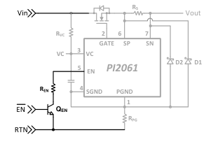
Figure 12: Enable circuit
Fault Indication: FT FT is an open collector output and its return is referenced to SGND. When the SGND pin is floating on a bias resistor (RPG) or in a constant current circuit, a level shift circuit can be added to create an output referenced to the system ground. See Figure 13.
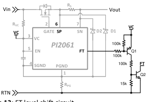
Figure 13: FT level shift circuit
Alternative Bias Circuit: Constant current circuit for high voltage application. In a wide operating input voltage range the size of RVC and RPG may be become large to support power dissipation. A simple constant current circuit, shown in Figure 14 can be used instead of RVC and RPG to allow the circuit to operate between 18V and 80V (100V/100ms transient) with low power dissipation components. Please refer to Picor application notes for more details on how to design a floating bias with the constant current circuit.
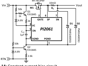
Figure 14: Constant current bias circuit
Page 10 of 16
Page 11
N-Channel MOSFET Selection: Several factors affect MOSFET selection including cost and following ratings; on-state resistance (RDS(on)), DC current, short pulse current, avalanche, power dissipation, thermal conductivity, drain-to-source breakdown voltage (BVDSS), gate-to-source voltage (VGS), and gate threshold voltage (VGS (TH)).
The first step is to select a suitable MOSFET based on the BVDSS requirement for the application. The BVDSS voltage rating should be higher than the applied Vin voltage plus expected transient voltages. Stray parasitic inductance in the circuit can also contribute to significant transient voltage condition, particularly during MOSFET turn-off after an over current fault has been detected.
In a disconnect switch application when the output is shorted, a large current is sourced from the power source through the MOSFET. Depending on the input impedance of the system, the current may get very high before the MOSFET is turned off. Make sure that the MOSFET pulse current capability can withstand the peak current. Also, such high current conditions will store energy even in a small parasitic inductance. The PI2061 has a very fast response time to terminate a fault condition achieving 120ns typical and 200ns maximum. This fast response time will minimize the peak current to keep stored energy and MOSFET avalanche energy very low to avoid damage (electrical stress) to the MOSFET.
Peak current during output short is calculated as follows, assuming that the input power source has very low impedance and it is not a limiting factor:
Where: : Peak current in the MOSFET right before it is turned off. : Input voltage at MOSFET drain before output short condition occurred. : Over current turn-off time. This will include PI2061 delay and the MOSFET turn off time. : Circuit parasitic inductance
The MOSFET avalanche energy during an input short is calculated as follows:
Where: : Avalanche energy : MOSFET breakdown voltage
MOSFET RDS(on) and maximum steady state power dissipation are closely related. Generally the lower the MOSFET RDS(on), the higher the current capability and the lower the resultant power dissipation for a given current. This leads to reduced thermal management overhead, but will ultimately be higher cost compared to higher RDS(on) parts. It is important to understand the primary design goal objectives for the application in order to effectively trade off the performance of one MOSFET versus another.
Power dissipation in load switch circuits is derived from the total drain current and the on-state resistance of the selected MOSFET.
MOSFET power dissipation:
Where : : MOSFET Drain Current : MOSFET on-state resistance
Note: In the calculation use RDS(on) at maximum MOSFET temperature because RDS(on) is temperature dependent. Refer to the normalized RDS(on) curves in the MOSFET manufacturer’s datasheet. Some MOSFET RDS(on) values may increase by 50% at 125°C compared to values at 25°C.
The Junction Temperature rise is a function of power dissipation and thermal resistance.
Where:
: MOSFET Junction-to-Ambient thermal resistance
Page 11 of 16
Page 12
Typical Application Example 1: 12V Load Switch
Requirement: Input Bus Voltage = 12V (±10% , 10.8V to 13.2V) Maximum Load Current = 10A Minimum Trip current = 12A Maximum Ambient Temperature = 75°C
Solution: PI2061 with a suitable external MOSFET should be used, configured as shown in the circuit schematic in .
Select a suitable N-Channel MOSFET: Most industry standard MOSFETs have a VGS rating of +/-12V or higher. Select an N-Channel MOSFET with a low RDS(on) which is capable of supporting the full load current with some margin, so a MOSFET capable of at least 18A in steady state is reasonable. An exemplary MOSFET having these characteristic is the Si4630DY from Siliconix.
From Si4630DY datasheet: N-Channel MOSFET VDS= 25V ID = 32A continuous drain current ID(Pulse) = 70A Pulsed drain current VGS(MAX)=±16V RθJA= 80°C/W under Steady State condition RDS(on)=2.2m typical and 2.7m maximum at ID=20A, VGS=10V, TJ=25°C
Select Sense Resistor:
Rs power dissipation at maximum operating current
Maximum trip current
Power dissipation: RDS(on) is 2.7m maximum at 25°C & 10 VGS and will increase as the temperature increases. Add 40°C to maximum ambient temperature to compensate for the temperature rise due to power dissipation. At 115°C (75°C + 40°C) RDS(on) will increase by 37%.
maximum at 115°C
Maximum Junction temperature
VC Bias: Vin maximum input is 13.2V, this is higher than the 11V VC minimum Clamp Voltage (VVC-SGND) minimum, but the minimum input voltage is greater than VVC-SGND minimum. Use 300 resistor for each RVC and RPG to minimize regulator clamp current.
Power dissipation of RVC and RPG:
Both resistors have very low power dissipation, less than 50mW. Any package size resistor, 0201 (0603 metric) or larger, can be used.
EN: Tie EN pin to VC since Enable function is always on.
FT: Fault function is not required, leave fault pin unconnected.
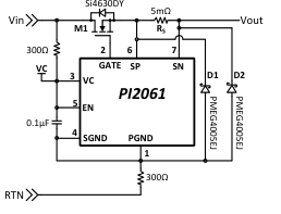
Figure 15: PI2061 in 12V Bus high side load switch application.
Page 12 of 16
Page 13
Typical application Example 2: Requirement: +48V Load Switch with Enable Function Bus Voltage = +48V (+36V to +55V) Maximum Load Current = 5A Minimum Trip current = 6A Maximum Ambient Temperature = 60°C
Solution: PI2061 with a suitable MOSFET should be used and configured as shown in Figure 16.
Select a suitable N-Channel MOSFET: Select a MOSFET with voltage rating higher than the input voltage, Vin, plus any expected transient voltages, with a low RDS(on) that is capable of supporting the full load current with margin. For instance, a 100V rated MOSFET with 10A current capability is suitable. An exemplary MOSFET having these characteristic is IRF7853PbF from International Rectifier.
From the IRF7853PbF datasheet: N-Channel MOSFET VDS= 100V ID = 8.3A maximum continuous drain current at 25°C ID-PULSE = 66A pulsed drain current VGS(MAX) =±20V RθJA= 50°C/W on 1in2 copper, t ≤ 10seconds RθJA for continuous operation not provided RDS(on)=14.4m typical at VGS=10V, TJ=25°C RDS(on)=18m maximum at VGS=10V, TJ=25°C
Select Sense Resistor:
Rs power dissipation at maximum operating current
Maximum trip current
Power dissipation: RDS(on) is 18m maximum at 25°C & 10 VGS and will increase as the temperature increases. Add 20°C to maximum ambient temperature to compensate for the temperature rise due to power dissipation. At 80°C (60°C + 20°C) RDS(on) will increase by 40%.
at maximum at 80°C
Maximum Junction temperature
Recalculate maximum RDS(on) at 95°C. At 95°C RDS(on) will increase by 50%:
at maximum at 95°C
Maximum Junction temperature after 10s
For continuous operation refer the MOSFET datasheet for RθJA under continuous operation and use in place of 50°C/W.
VC Bias Resistors:
Select 7.5k resistor
Select 10k resistor
Power dissipation of RVC and RPG:
Recommended Schottky: PMEG4005EJ from NXP or equivalent
Page 13 of 16
Page 14
Enable Input Circuit: EN Pull EN pin to ground (return) to disable. This can be accomplished with a signal transistor (Q1) in open collector configuration and a pull-up resistor REN.
A 5% 360k resistor can be used to pull down on EN pin. Note that the control signal phase is inverted.
Layout Recommendation:
Use the following general guidelines when designing printed circuit boards. An example of the typical land pattern for the PI2061 is shown in Figure 17.
Use a solid ground (return) plane to reduce circuit parasitics. Connect Rs terminal at SP pin side, D1 cathode and all MOSFET source pins together with a wide trace to reduce trace parasitics and to accommodate the high current output. Connect Rs terminal at SN pin side to the load with a wide trace. Also connect all MOSFET drain pins together with a wide trace to accommodate the high current input Kelvin connect SP pin and SN pin to Rs terminals. The VC bypass capacitor should be located as close as possible to the VC and SGND pins. Place the PI2061 and VC bypass capacitor on the same layer of the board. The VC pin and CVC PCB trace should not contain any vias.
Dedicate a small copper area on lower layer underneath the controller for PGND and SGND to make a single point connection and simplify layout inter connect. Make sure that Vin to Vout current
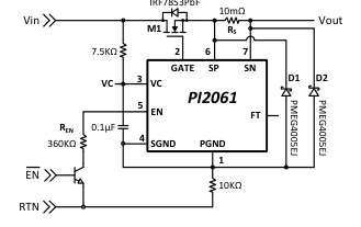
Figure 16: PI2061 in high side +48V application, VC is biased through a bias resistor
return path is solid underneath the MOSFET (M1) and the sense resistor (R1). Make sure D1 and D2 connecting traces are very short to reduce parasitic inductance that might produce voltage drop due MOSFET fast turn off. Use 1oz of copper or thicker if possible to reduce trace resistance and power dissipation.
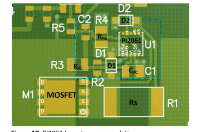
Figure 17: PI2061 layout recommendation
Page 14 of 16
Page 15
Package Drawings:
10 Lead DFN
| Ordering Information | ||
| Part Number | Package | Transport Media |
| PI2061-00-QEIG | 3mm x 3mm 10 Lead DFN | T&R |
Page 15 of 16
Page 16
Warranty
Vicor products are guaranteed for two years from date of shipment against defects in material or workmanship when in normal use and service. This warranty does not extend to products subjected to misuse, accident, or improper application or maintenance. Vicor shall not be liable for collateral or consequential damage. This warranty is extended to the original purchaser only.
EXCEPT FOR THE FOREGOING EXPRESS WARRANTY, VICOR MAKES NO WARRANTY, EXPRESS OR LIMITED, INCLUDING, BUT NOT LIMITED TO, THE WARRANTY OF MERCHANTABILITY OR FITNESS FOR A PARTICULAR PURPOSE.
Vicor will repair or replace defective products in accordance with its own best judgment. For service under this warranty, the buyer must contact Vicor to obtain a Return Material Authorization (RMA) number and shipping instructions. Products returned without prior authorization will be returned to the buyer. The buyer will pay all charges incurred in returning the product to the factory. Vicor will pay all reshipment charges if the product was defective within the terms of this warranty.
Information published by Vicor has been carefully checked and is believed to be accurate; however, no responsibility is assumed for inaccuracies. Vicor reserves the right to make changes to any products without further notice to improve reliability, function, or design. Vicor does not assume any liability arising out of the application or use of any product or circuit; neither does it convey any license under its patent rights nor the rights of others. Vicor general policy does not recommend the use of its components in life support applications wherein a failure or malfunction may directly threaten life or injury. Per Vicor Terms and Conditions of Sale, the user of Vicor components in life support applications assumes all risks of such use and
indemnifies Vicor against all damages.
Vicor’s comprehensive line of power solutions includes high density AC-DC and DC-DC modules and accessory components, fully configurable AC-DC and DC-DC power supplies, and complete custom power systems.
Information furnished by Vicor is believed to be accurate and reliable. However, no responsibility is assumed by Vicor for its use. Vicor components are not designed to be used in applications, such as life support systems, wherein a failure or malfunction could result in injury or death. All sales are subject to Vicor’s Terms and Conditions of Sale, which are available upon request.
Specifications are subject to change without notice.
Vicor Corporation 25 Frontage Road Andover, MA 01810 USA
Picor Corporation 51 Industrial Drive North Smithfield, RI 02896 USA
Customer Service: custserv@vicorpower.com Technical Support: apps@vicorpower.com Tel: 800-735-6200 Fax: 978-475-6715
Page 16 of 16