


 Download PDF
PI1004-1 VICOR
Document overview
- PDF pages: 16
Technical content
Page 1
PI1004-1 PI1004-2
Programmable Point-of-Load Controller with 6-bit VID
Description
The PI1004 IC combines a Voltage Identification Digital Input (VID) controlled reference with control and supervisory functions to accurately set the regulator output voltage at the point of load, for isolated and CPU DC-DC converters in desktop and server applications. The PI1004 feature set is intended to be used in conjunction with a variety of power architectures, including Factorized Power Architecture (FPA), to provide CPU power in accordance with Intel® VR10.X requirements. The feature set includes a precision error amplifier for remote differential sensing of the output voltage, a six bit programmable VID reference voltage output with 12.5 mV resolution, and flexible adaptive voltage positioning.
The regulation voltage can also be shifted below the VID range with a programmable offset current. The controller includes an over-voltage indicator output, an open collector power-good output, under-voltage lockout and an externally programmable soft start.
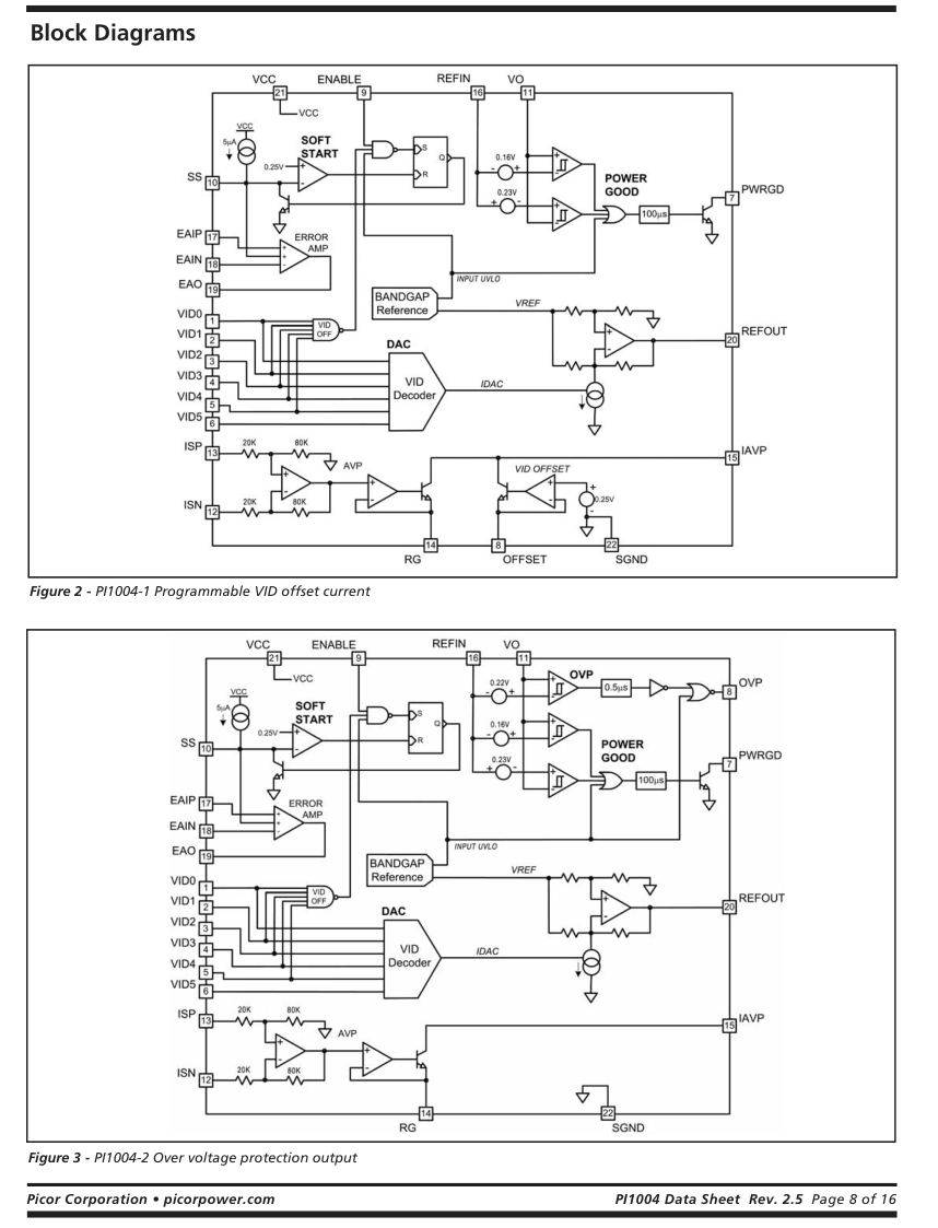
The PI1004 is available in two options; PI1004-1: Programmable VID offset current and no OVP output. The VID offset current is used to create an offset to the DAC output. PI1004-2: OVP output and no VID offset.
Typical Circuit
Features
- 0.5% Typical initial output voltage accuracy
- Remote differential output voltage sense
- 6 Bit DAC, with 12.5 mV resolution
- 5 V to 12 V Operation
- Power good output with blanking
- Programmable adaptive voltage positioning (AVP)
- Over voltage protection (OVP) output or programmable VID offset
- Programmable soft start
- Optimized for VRM/VRD 10.X specifications
- 20 MHz Gain bandwidth amplifier
- Enable input
Applications
- Supports FPA
- Intel® VR10.X CPU Power
- Workstation CPU Power
- Isolated DC-DC Converters
Package
- 24-Lead (4mm x 4mm) QFN
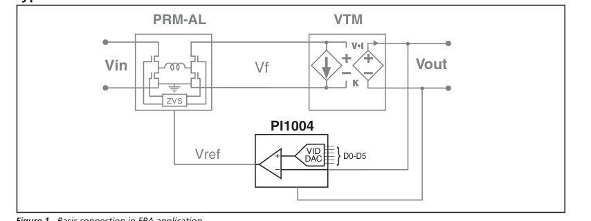
Figure 1 - Basic connection in FPA application.
PI1004 Data Sheet Rev. 2.5 Page 1 of 16
Page 2
| Pin Description | ||
|---|---|---|
| PIN # | Pin Name | Description |
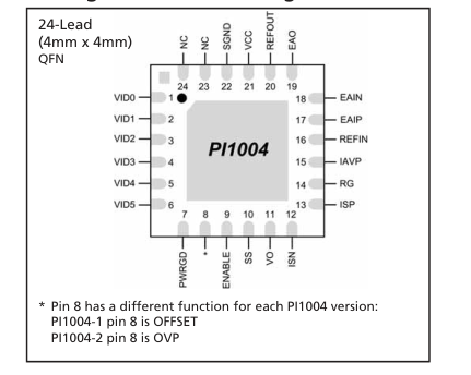
| 1- 6 | VID[0:5] | Voltage identification digital inputs. The VID inputs program the reference voltage on the REFOUT pin. Tying all VID pins high is treated as a fault and sets the fault latch. To hardwire the VID code, the inputs may be connected to Vcc or SGND as applicable. See Table 1 for VID codes. |
| 7 | PWRGD | Power-good open-collector output. This pin is an open circuit when (REFIN-230 mV) ≤VO ≤(REFIN+160 mV) and the input bus voltage is not in a UVLO condition. When VO is outside the VO window, (REFIN- 230 mV ) < VO < (REFIN+160 mV) or the input bus voltage is in a UVLO condition, or if the ENABLE is low, the PWRGD output is low. |
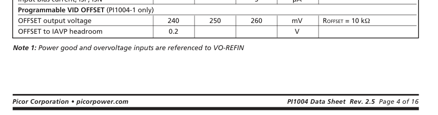
| 8 | OFFSET | PI1004-1 only. Provides a programmable VID offset current. A current equal to the current out of the OFFSET pin is added to IAVP to provide a fixed negative offset. To program the offset connect a resistor between OFFSET and SGND. The current is nominally equal to 0.25 V / ROFFSET. Not used tie to Vcc. |
| 8 | OVP | PI1004-2 only. Over-voltage protection signal, TTL output. When VO ≥(REFIN+220 mV) and the input bus voltage is not in a UVLO condition and ENABLE is high, OVP is high. When VO < (REFIN+220 mV) or the input bus voltage is in a UVLO condition, or ENABLE is low, OVP is low. |
| 9 | ENABLE | Logic input control of biasing. If ENABLE = low the PI1004 is disabled and quiescent current is reduced to <400 uA. If ENABLE = high the PI1004 is enabled and the part operates normally if Vcc > UVLO. |
| 10 | SS | Soft start programming terminal. The error amp non-inverting input (EAIP) is clamped below the level of the SS pin. An internal 5uA charging current is provided to program soft start with an external capacitor. Soft start pin is discharged and held low with ENABLE low, UVLO, or VID=x11111. To control soft-start connect a capacitor between the SS pin and SGND. |
| 11 | VO | Output voltage positive sense signal used for the power good and over-voltage protection circuits. Connect directly to the output or if feedback divider is employed, connect to the output through a voltage divider with the same ratio as the feedback divider. |
| 12 | ISN | Load current negative sense terminal. Connect ISN to the negative side of the sense resistor. If AVP is not used, tie ISN to SGND. |
| 13 | ISP | Load current positive sense terminal. Connect ISP to the positive side of the sense resistor to detect load current for AVP. If AVP is not used, tie ISP to SGND. |
| 14 | RG | Adaptive voltage positioning gain resistor connection. The sink current from the IAVP pin is: IAVP = 4*[V(ISP)-V(ISN)]/RG. If AVP is not used, tie RG to Vcc. |
| 15 | IAVP | Adaptive voltage positioning sink current. This pin sinks current proportional to the load. Connect to the EAIP pin with an AVP resistor (RAVP) tied from EAIP to REFOUT. The regulator output voltage will drop with increasing load. If AVP is not used, connect IAVP to Vcc. |
| 16 | REFIN | Reference input voltage for the over-voltage protection and power good indicators. Normally REFIN is tied to REFOUT. |
| 17 | EAIP | Non-inverting input to the error amplifier. If AVP and offset are not used, connect EAIP to REFOUT. To use AVP connect directly to IAVP and to REFOUT through a resistor. |
| 18 | EAIN | Inverting input to the error amplifier. Connect EAIN to the positive remote output voltage sense point through the feedback network. Run in parallel to the SGND connection to avoid noise pick-up. |
| 19 | EAO | Error amplifier output terminal. |
| 20 | REFOUT | Reference output voltage as defined by the VID codes in Table 1. The reference is capable of sourcing up to 1 mA of current. In a typical CPU application REFOUT is connected to REFIN to set the thresholds for Power Good and to EAIP through a resistor to enable Adaptive Voltage Positioning. |
| 21 | VCC | Internal circuit supply. Bypass Vcc to SGND with a 0.1 µF capacitor. |
| 22 | SGND | Internal substrate connection and negative output voltage sense terminal. Connect to the negative remote output voltage sense point and run in parallel with the positive sense line to avoid noise pick-up. |
| 23,24 | NC | No connect. Post package programming pin. |
| Picor Corporation • picorpower.com PI1004 Data Sheet Rev. 2.5 Page 2 of 16 | ||
Page 3
Absolute Maximum Ratings
Package Connection Diagram
These are stress ratings only and functional operation of the device at these ratings is not implied. Exposure to absolute maximum rating conditions for extended periods of time may affect reliability.
Vcc, EAO........................................-0.3 V to 16 V / 20 mA OVP ...............................................-0.3 V to 16 V / 10 mA VID5:0, ENABLE, SS, ISN, ISP, RG, IAVP, EAIP, EAIN, REFOUT, OFFSET...................-0.3 V to 16 V / 1 mA PWRGD, ......................................-0.3 V to 5.5 V / 10 mA REFIN, VO,.....................................-0.3 V to 5.5 V / 1 mA SGND.......................................................................20 mA Storage Temperature .............................-65 °C to 150 °C ESD Sensitivity Class Rating.........................................1 C Soldering Temp. IR or Convection (20 sec) 3 pg 15....250 °C
Electrical Specifications
Unless otherwise specified: -40°C < Tj < 125 °C, 4.5V < VCC < 13.2V
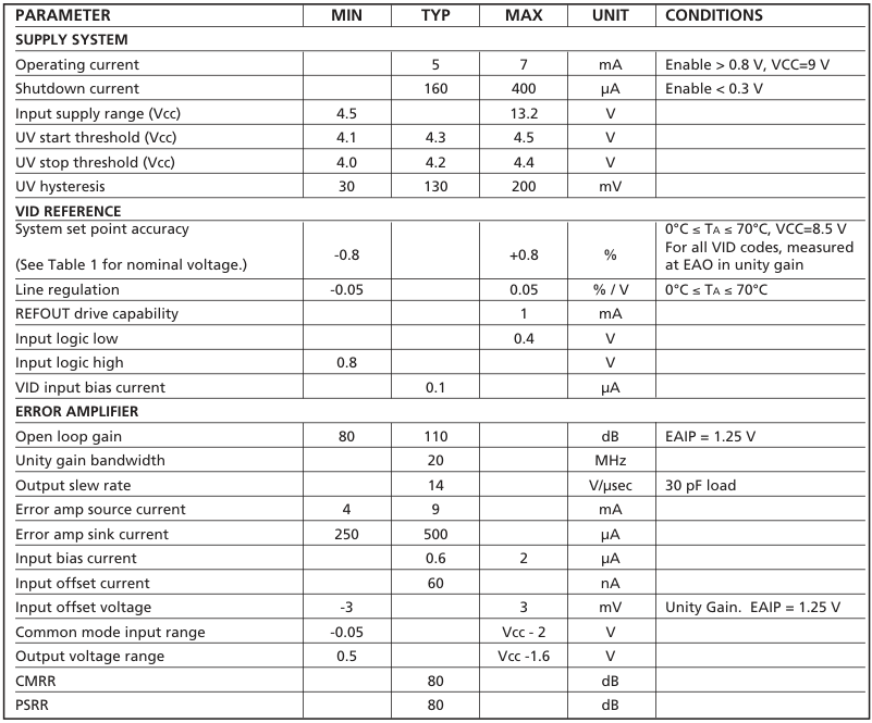
| 5 | 7 | mA | Enable > 0.8 V, VCC=9 V | |
| 160 | 400 | µA | Enable < 0.3 V | |
| 4.5 | 13.2 | V | ||
| 4.1 | 4.3 | 4.5 | V | |
| 4.0 | 4.2 | 4.4 | V | |
| 30 | 130 | 200 | mV |
| -0.8 | +0.8 | % | 0°C ≤TA ≤70°C, VCC=8.5 V For all VID codes, measured at EAO in unity gain | |
|---|---|---|---|---|
| -0.05 | 0.05 | % / V | 0°C ≤TA ≤70°C | |
| 1 | mA | |||
| 0.4 | V | |||
| 0.8 | V | |||
| 0.1 | µA |
PI1004 Data Sheet Rev. 2.5 Page 3 of 16
Page 4

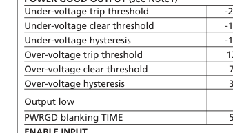
| -280 | -230 | -185 | mV | 0°C ≤TA ≤70°C |
| -185 | -150 | -100 | mV | 0°C ≤TA ≤70°C |
| -100 | - 80 | -50 | mV | 0°C ≤TA ≤70°C |
| 125 | 160 | +185 | mV | 0°C ≤TA ≤70°C |
| 75 | 110 | +135 | mV | 0°C ≤TA ≤70°C |
| 35 | 50 | 80 | mV | 0°C ≤TA ≤70°C |
| 0.4 | V | IPWRGD = 4 mA (Enabled) IPWRGD = 250 µA (Disabled) | ||
| 50 | 100 | 300 | µsec |
ENABLE INPUT
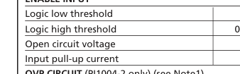
| 0.3 | V | |||
| 0.8 | V | 0°C ≤TA ≤70°C | ||
| 1.8 | V | |||
| 2 | µA |
OVP CIRCUIT (PI1004-2 only) (see Note1)
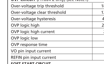
| 180 | 220 | 250 | mV | 0°C ≤TA ≤70°C |
| 120 | 150 | 180 | mV | 0°C ≤TA ≤70°C |
| 40 | 70 | 100 | mV | 0°C ≤TA ≤70°C |
| 2.5 | 3.5 | 4.5 | V | Iovp = -2 mA |
| 2 | 4.5 | mA | ||
| 0.4 | V | Iovp = 0.5 mA | ||
| 0.5 | µsec | |||
| 0.25 | 0.6 | µA | ||
| 0.25 | 0.6 | µA |
SOFT START CIRCUIT
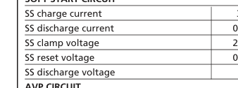
| 3 | 5 | 7 | µA | 0°C ≤TA ≤70°C |
| 0.2 | 0.7 | mA | ||
| 2.3 | 2.6 | 2.9 | V | |
| 0.2 | 0.25 | 0.3 | V | |
| 0.1 | V |
AVP CIRCUIT
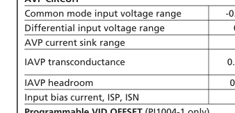
| -0.05 | 0.4 | V | ||
| 0 | 135 | mV | ||
| 200 | µA | |||
| 0.97 | 1.00 | 1.03 | mS | RG=4 kΩ, ISP = 135 mV ISN = 0V |
| 0.2 | V | |||
| 5 | µA |
Page 5
| VID Pins (0 = low, 1 = high) | 1 (EAO) 0.8375 | VID Pins (0 = low, 1 = high) | 1 (EAO) 1.2125 | |||||||||||
| VID5 | VID4 | VID3 | VID2 | VID1 | VID0 | VID5 | VID4 | VID3 | VID2 | VID1 | VID0 | |||
| 0 | 0 | 1 | 0 | 1 | 0 | 0 | 1 | 1 | 0 | 1 | 0 | |||
| 1 | 0 | 1 | 0 | 0 | 1 | 0.8500 | 1 | 1 | 1 | 0 | 0 | 1 | 1.2250 | |
| 0 | 0 | 1 | 0 | 0 | 1 | 0.8625 | 0 | 1 | 1 | 0 | 0 | 1 | 1.2375 | |
| 1 | 0 | 1 | 0 | 0 | 0 | 0.8750 | 1 | 1 | 1 | 0 | 0 | 0 | 1.2500 | |
| 0 | 0 | 1 | 0 | 0 | 0 | 0.8875 | 0 | 1 | 1 | 0 | 0 | 0 | 1.2625 | |
| 1 | 0 | 0 | 1 | 1 | 1 | 0.9000 | 1 | 1 | 0 | 1 | 1 | 1 | 1.2750 | |
| 0 | 0 | 0 | 1 | 1 | 1 | 0.9125 | 0 | 1 | 0 | 1 | 1 | 1 | 1.2875 | |
| 1 | 0 | 0 | 1 | 1 | 0 | 0.9250 | 1 | 1 | 0 | 1 | 1 | 0 | 1.3000 | |
| 0 | 0 | 0 | 1 | 1 | 0 | 0.9375 | 0 | 1 | 0 | 1 | 1 | 0 | 1.3125 | |
| 1 | 0 | 0 | 1 | 0 | 1 | 0.9500 | 1 | 1 | 0 | 1 | 0 | 1 | 1.3250 | |
| 0 | 0 | 0 | 1 | 0 | 1 | 0.9625 | 0 | 1 | 0 | 1 | 0 | 1 | 1.3375 | |
| 1 | 0 | 0 | 1 | 0 | 0 | 0.9750 | 1 | 1 | 0 | 1 | 0 | 0 | 1.3500 | |
| 0 | 0 | 0 | 1 | 0 | 0 | 0.9875 | 0 | 1 | 0 | 1 | 0 | 0 | 1.3625 | |
| 1 | 0 | 0 | 0 | 1 | 1 | 1.0000 | 1 | 1 | 0 | 0 | 1 | 1 | 1.3750 | |
| 0 | 0 | 0 | 0 | 1 | 1 | 1.0125 | 0 | 1 | 0 | 0 | 1 | 1 | 1.3875 | |
| 1 | 0 | 0 | 0 | 1 | 0 | 1.0250 | 1 | 1 | 0 | 0 | 1 | 0 | 1.4000 | |
| 0 | 0 | 0 | 0 | 1 | 0 | 1.0375 | 0 | 1 | 0 | 0 | 1 | 0 | 1.4125 | |
| 1 | 0 | 0 | 0 | 0 | 1 | 1.0500 | 1 | 1 | 0 | 0 | 0 | 1 | 1.4250 | |
| 0 | 0 | 0 | 0 | 0 | 1 | 1.0625 | 0 | 1 | 0 | 0 | 0 | 1 | 1.4375 | |
| 1 | 0 | 0 | 0 | 0 | 0 | 1.0750 | 1 | 1 | 0 | 0 | 0 | 0 | 1.4500 | |
| 0 | 0 | 0 | 0 | 0 | 0 | 1.0875 | 0 | 1 | 0 | 0 | 0 | 0 | 1.4625 | |
| 1 | 1 | 1 | 1 | 1 | 1 | OFF2 | 1 | 0 | 1 | 1 | 1 | 1 | 1.4750 | |
| 0 | 1 | 1 | 1 | 1 | 1 | OFF2 | 0 | 0 | 1 | 1 | 1 | 1 | 1.4875 | |
| 1 | 1 | 1 | 1 | 1 | 0 | 1.1000 | 1 | 0 | 1 | 1 | 1 | 0 | 1.5000 | |
| 0 | 1 | 1 | 1 | 1 | 0 | 1.1125 | 0 | 0 | 1 | 1 | 1 | 0 | 1.5125 | |
| 1 | 1 | 1 | 1 | 0 | 1 | 1.1250 | 1 | 0 | 1 | 1 | 0 | 1 | 1.5250 | |
| 0 | 1 | 1 | 1 | 0 | 1 | 1.1375 | 0 | 0 | 1 | 1 | 0 | 1 | 1.5375 | |
| 1 | 1 | 1 | 1 | 0 | 0 | 1.1500 | 1 | 0 | 1 | 1 | 0 | 0 | 1.5500 | |
| 0 | 1 | 1 | 1 | 0 | 0 | 1.1625 | 0 | 0 | 1 | 1 | 0 | 0 | 1.5625 | |
| 1 | 1 | 1 | 0 | 1 | 1 | 1.1750 | 1 | 0 | 1 | 0 | 1 | 1 | 1.5750 | |
| 0 | 1 | 1 | 0 | 1 | 1 | 1.1875 | 0 | 0 | 1 | 0 | 1 | 1 | 1.5875 | |
| 1 | 1 | 1 | 0 | 1 | 0 | 1.2000 | 1 | 0 | 1 | 0 | 1 | 0 | 1.6000 | |
Table 1. Voltage Identification
Table 1 NOTES: 1. (EAO) is equal to the maximum output voltage specified by the Intel design guide, Voltage Regulator-Down (VRD) 10.0, February 2004.
- EAO is held low during VID OFF codes.
PI1004 Data Sheet Rev. 2.5 Page 5 of 16
Page 6
Functional Description
The block diagram in Figure 2 shows that the PI1004-1 has a programmed VID offset function and no OVP function. Figure 3 shows the PI1004-2 with the OVP function in place of the VID offset. Unless otherwise stated please refer to Figure 2 and application diagram Figure 4a for the following description.
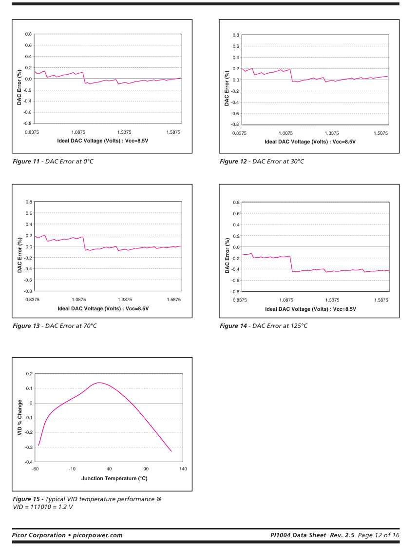
Voltage identification and Reference Out The REFOUT output pin provides a scaled temperature stable reference voltage (see temperature curves in figure 15) that is incremented by the VID input state decoding and DAC (digital to analog converter) function. The 6 bit DAC provides a minimum increment resolution of 12.5mV. The VR10.X VID code accuracy shown in Table 1 is measured at the output of the error amp in the unity gain buffer configuration.
REFOUT will be determined by VID[5:0] according to the Intel VR10.X Voltage Identification Table. In a typical CPU application using AVP (Adaptive Voltage Positioning) REFIN is tied directly to REFOUT and EAIP is tied to REFOUT through a resistor for AVP adjustment. VID = x1111 is treated as a fault and sets the Fault Latch function that will be explained further in the other sections.
Current Sensing and AVP Pins ISN and ISP form the input to a differential voltage sense amplifier that can be used for current sensing and adaptive voltage positioning (AVP). The amplifier has a narrow common mode input range for ground reference voltages.
The AVP amplifier has a fixed gain of 4 to amplify the voltage across a sense resistor that is representative of the load current. The output voltage of the amplifier is fed to a unity gain buffer and impressed across the external RG resistor converting the voltage to a current that is reflected as a sink current at the IAVP pin 15.
INPUTS
ENABLE
UVLO
VID[5:0]
OVP
L
X
X
L
H
H
X
L
H
VID Valid
Active
H
L VID Valid
Active
H
L
X11111
Active The PI-1004-1 has a second voltage to current converter to create the OFFSET function with a fixed reference voltage of 250mV that is impressed across an external ROFFSET resistor. This voltage to current conversion reflects a fixed sink current at the IAVP pin. The sum of these two currents flows through the external resistor, RAVP when connected as shown in figure 4a completing the adaptive and offset functions. The control error amplifier input voltage will be dependent on the reference determined by the VID input state, minus any programmed offset voltage, minus the AVP correction for load setting the slope of the load line.
The IAVP pin is set up to provide a current proportional to the load current. Various load lines can be selected by choosing values of the output current shunt resistor, RG and the resistor between REFOUT and EAIP (RAVP) for the proper droop. The value of the current shunt should be chosen for a voltage drop of 135mV or slightly lower at full load.
Differential Output Voltage Sense The core control error amplifier has two non-inverting inputs to accommodate a soft start feature. With the proper non-faulted conditions the soft-start charging current of 5uA will be sourced out of the SS pin to an external capacitor. This feature provides the ability to control the rate of rise in the output voltage up to the point of regulation. The fault conditions are defined in the fault circuitry section and listed in Table 2. If a fault condition exits the internal sink transistor will hold the SS pin to the signal ground potential. Recovery from any of the fault conditions will result in a full soft-start interval.
The lower of the two non-inverting inputs of the error amplifier will dominate. When all faults are cleared the SS input provides the dominant ramping input voltage until it exceeds the EAIP reference. The SS input continues to ramp to the soft-start clamp voltage while the EAIP
OUTPUTS
PWRGD
REFOUT
EAO
SS
L
L
L
L
(Limited drive)
L
≤ VID
L
L
Active
VID
Active
VID
Active
H
Active
VID
L
L
ENABLE Low = Off UVLO High = VCC is low OVP High = Fault PWRGD Low = Fault VID = See VID Table 1
Table 2. I/O Functional States
PI1004 Data Sheet Rev. 2.5 Page 6 of 16
Page 7
becomes the control reference. The amplifier EAIN inverting input and the EAO output pin can be configured as a unity gain follower or as an inverting amplifier with the proper feedback components to set the close loop gain and frequency response of the voltage control loop.
Differential sensing is accomplished by referencing the entire PI1004 to the negative return of the load (typically CPUVSS). The SGND pin serves a dual purpose of returning the PI1004 VCC current and sensing the low side of the load. The internal reference "rides" on SGND to compensate for voltage changes at the load. Special care must be taken in the layout to avoid noise pick-up or offsets due to ground loop currents.
Fault Circuitry There are three input conditions that will set the fault latch determined by ENABLE, VIDOFF or UVLO states as shown in Table 2. Any fault will clamp the non-inverting error amp input (EAIP) and SS pin to SGND. The fault latch is reset when the SS pin drops below 0.25 V AND all faults are cleared at the Set dominant latch input.
Power Good and Over-Voltage Protection The PWRGD and OVP (OVP in PI1004-2 only) pins provide output signals when the output voltage exceeds internally set thresholds. The inputs to the PWRGD and OVP comparators are referenced to REFIN and VO. The PWRGD and OVP signals are outputs for system use and do not trigger an internal fault.
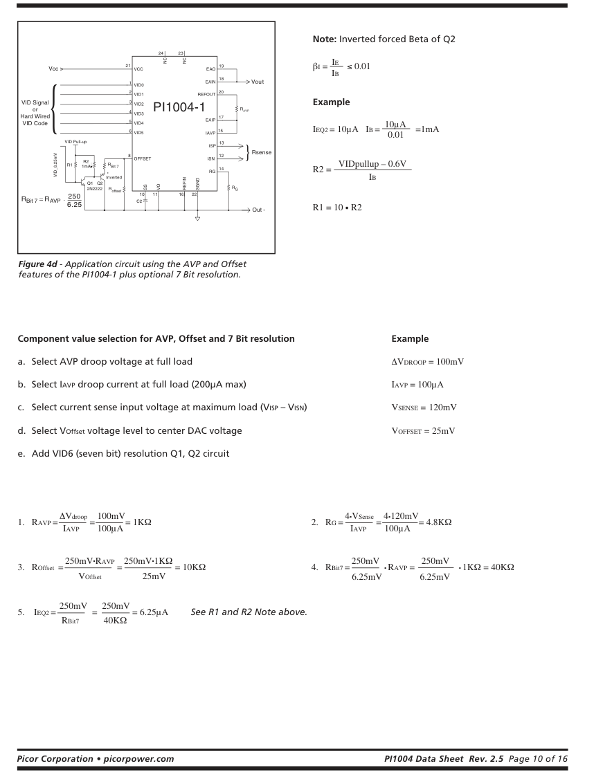
Programmable VID Offset REFOUT is set to the VR10 maximum output voltage according to Table 1. For PI1004-1, the no-load VID output voltage can be reduced to accommodate various load line tolerance bands with the OFFSET function. Once the value of RAVP has been chosen for the desired load line, ROFFSET can be selected for the required no-load offset. Refer to Figure 4d to determine resistor values setting the AVP and Offset parameters.
Figures 5-10 demonstrate some of the dynamic performance of these functions such as AVP response time, REFOUT response to VID change, VID blanking interval, error amplifier unity gain slew rate and soft-start response to stepped Vcc in that order. Figures 11-14 demonstrate typical DAC error performance at specific temperatures and Figure 15 demonstrates the VID performance from -55 to 125 degrees Celsius at VID=1.2V.
Applications Description
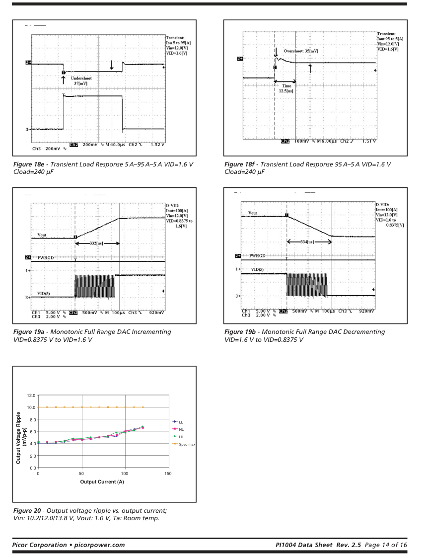
The PI1004 products were developed to enable Vicor’s FPA (Factorized Power Architecture) to meet Intel’s requirements defined in VRM/VRD 10.X specifications. A simplified schematic representation of this topology is shown in Figure 4a. DC Performance data of this configuration using the PI1004-1 is shown in Figures 16-17 and dynamic performance is shown in Figures 18a-g, 19a-b and 20.
In addition to FPA applications, independent functions of the PI1004 can be used in different combinations as building blocks in control applications.
The PI-1004 can be used as a VID controlled reference in an embedded power converter circuit. The PI1004 error amp can be configured as a unity gain buffer to provide the VRD capable reference to the non-inverting input to the control amp. If AVP is required, a method for sensing the load current would need to be implemented.
In isolated applications as shown in Figure 4b, the reference and error amplifier might replace a TL431 (Vcc power is required for the PI1004) while the PWRGD, OVP and AVP blocks replace a quad comparator. The PI1004 is a candidate for any application that uses a reference and several amplifiers or comparators especially where digital or hard-wire setting of voltages can be accommodated.
The IC can be used as a programmable reference control for a converter or power supply with a positive reference based trim configuration as shown in Figure 4c. For these applications a programmable output voltage and overvoltage features can be created using the error amp as a buffer creating a VR10 reference for the SC/trim input of the converter. Care must be taken not to exceed the amplifier output sink and source current capabilities and to be compatible with the converter reference pin.
The AVP block of circuits can be used to create two independent voltage to current converters providing a sink current that is the sum of the two at the IAVP pin. Again consideration of the specified range for these functions is required.
Finally the Power Good block can be used as basic comparators for voltage monitoring with the addition of an independent output on the OVP pin in the PI1004-2
An additional bit of resolution can be added to the DAC by using the circuit shown in Figure 4d with proper sequencing by the microprocessor 6.25 mV increments are possible.
PI1004 Data Sheet Rev. 2.5 Page 7 of 16
Page 8
Page 9
Application Diagrams
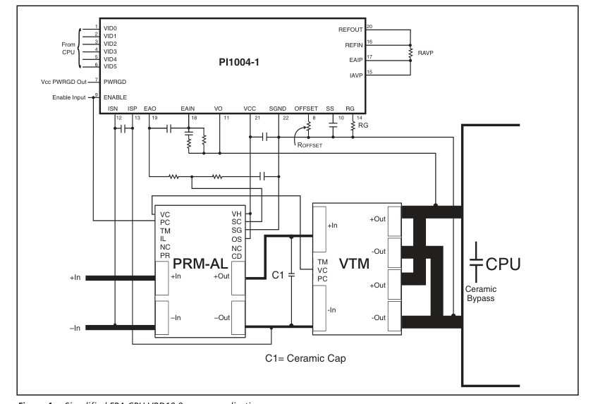
Figure 4a - Simplified FPA CPU VRD10.0 power application.
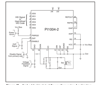
Figure 4b - Embedded Isolated Power Converter Application using the PI1004-2.
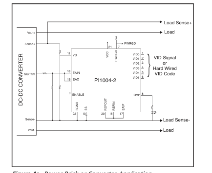
Figure 4c - Power Brick or Converter Application using the PI1004-2.
PI1004 Data Sheet Rev. 2.5 Page 9 of 16
Page 10
Page 11
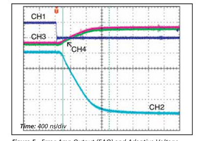
Figure 5 - Error Amp Output (EAO) and Adaptive Voltage Positioning (AVP) response to negative step. Error amp unity gain. ISN grounded, RAVP=1 K, RG=4 K CH1: ISP 200 mV/div
CH3: EAO 200 mV/div
CH2: RG 200 mV/div
CH4: EAIP 200 mV/div
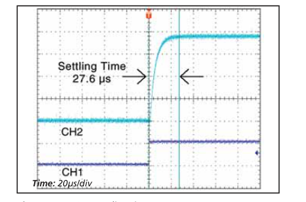
Figure 7 - REFOUT settling time CH1: VID4, 5 V/div CH2: REFOUT; 100 mV/div
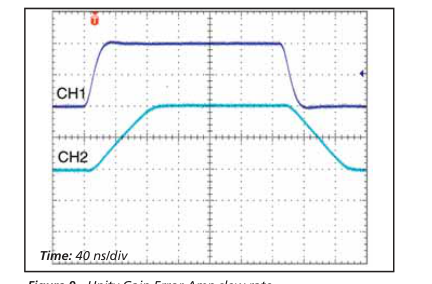
Figure 9 - Unity Gain Error Amp slew rate CH1: EAIP; 500 mV/div CH2: EAO; 500 mV/div
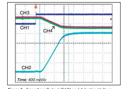
Figure 6 - Error Amp Output (EAO) and Adaptive Voltage Positioning (AVP) response to positive step. Error amp unity gain. ISN grounded, RAVP=1 K, RG=4 K CH1: ISP 200 mV/div
CH3: EAO 200 mV/div
CH2: RG 200 mV/div
CH4: EAIP 200 mV/div
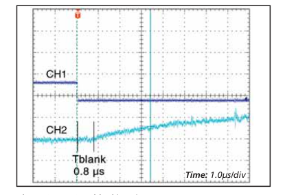
Figure 8 - REFOUT blanking time CH1: VID5, 5 V/div CH2: REFOUT; 100 mV/div
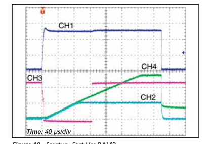
Figure 10 - Startup, Fast Vcc RAMP CH1: VCC; 2 V/div
CH3: PWRGD; 2 V/div
CH2: EAO; 1 V/div
CH4: SS; 1 V/div
PI1004 Data Sheet Rev. 2.5 Page 11 of 16
Page 12
Page 13
Application Measurements Using Fig. 4a
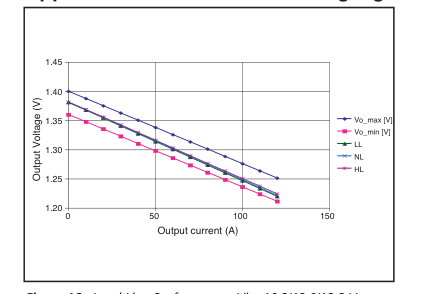
Figure 16 - Load Line Performance; Vin: 10.2/12.0/13.8 V, Vout: 1.4 V, Ta: Room temp
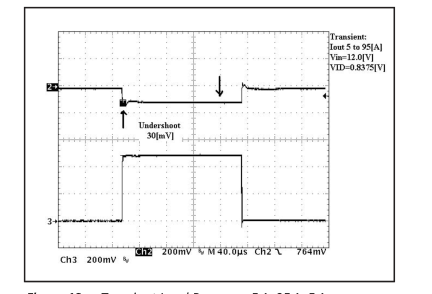
Figure 18a - Transient Load Response 5 A–95 A–5 A VID=0.8375 Cload=240 µF
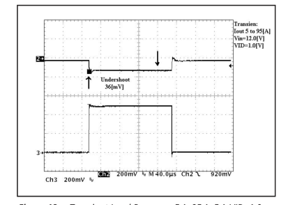
Figure 18c - Transient Load Response 5 A–95 A–5 A VID=1.0 Cload=240 µF
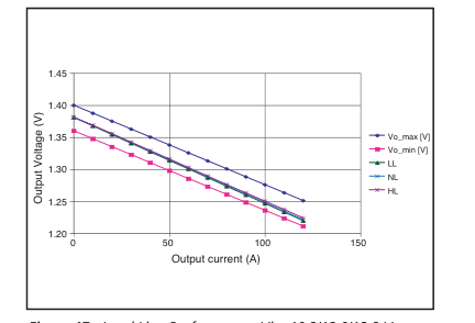
Figure 17 - Load Line Performance; Vin: 10.2/12.0/13.8 V, Vout: 1.4 V, Tj: 100°C
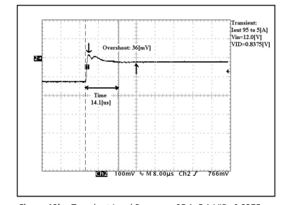
Figure 18b - Transient Load Response 95 A–5 A VID=0.8375 Cload=240 µF
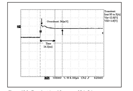
Figure 18d - Transient Load Response 95 A–5 A VID=1.0 Cload=240 µF
PI1004 Data Sheet Rev. 2.5 Page 13 of 16
Page 14
Page 15
Package Description
Layout Guidelines
Good layout technique is required for systems that combine sensitive amplifiers and switching converters. Extra care must be taken to provide high
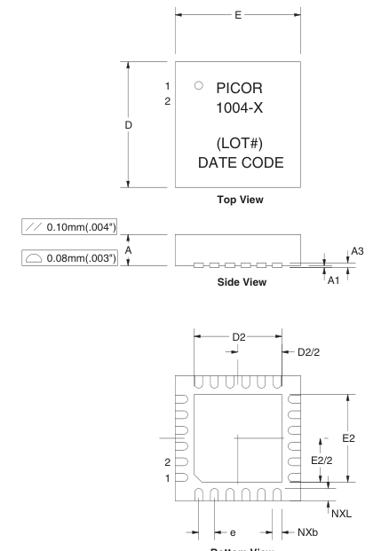
Bottom View
Thermal Resistance Ratings
PARAMETER
Maximum Junction-to-Ambient 2 Maximum Junction-to-Case
Ordering Information
PART NUMBER
PACKAGE
PI1004-1-QAHG
24 lead (4mm x 4mm) QFN
PI1004-2-QAHG 24 lead (4mm x 4mm) QFN
Note 2: In accordance with JEDEC JESD 51-5
frequency decoupling and to avoid introducing noise at sensitive nodes.
- The capacitors for VCC decoupling and Soft Start should provide low impedance paths to each pin and be referenced to SGND close to the PI1004.
- The connections from load VSS to SGND and the load VCC to EAIP form an output voltage sense pair and should be routed in parallel to avoid noise pick-up. If the layout allows PI1004 return current to flow through the load VSS to SGND connection, trace resistance must be considered to avoid an excessive offset voltage within the trace.
- The PI1004 EA integrator capacitor should be routed in a short loop to minimize noise pick-up.
- RG and ROFFSET should be tied to SGND near the PI1004 to avoid noise pickup.
| DIM | MILLIMETERS | INCHES |
| MIN NOM MAX | MIN NOM MAX | |
| A | 0.80 0.85 .90 | .031 .033 .035 |
| A1 | 0.00 0.02 0.05 | .000 .001 .002 |
| A3 | -- 0.20ref -- | -- .008 ref -- |
| NXb | 0.20 0.25 0.30 | .008 .010 .012 |
| D | 4.00 | .157 |
| D2 | 2.70 2.80 2.90 | .106 .110 .114 |
| E | 4.00 | .157 |
| E2 | 2.70 2.80 2.90 | .106 .110 .114 |
| e | 0.50 | .020 |
| NXL | 0.30 0.40 0.50 | .012 .016 .020 |
Controlling Dimensions: Millimeters
SYMBOL
TYPICAL
UNIT
46
°C/W
θJA
2
°C/W
θJC
BRANDING
TEMP. RANGE
TRANSPORT MEDIA
1004-1
-40°C to 125°C
T&R
1004-2
-40°C to 125°C
T&R
Note 3: This product is MSL classified at the peak soldering reflow temperature listed in the Absolute Maximum Rating section to meet the lead free requirements of the joint IPC® and JEDEC® standard J-STD-020C.
PI1004 Data Sheet Rev. 2.5 Page 15 of 16
Page 16
Vicor’s comprehensive line of power solutions includes high-density AC-DC & DC-DC modules and accessory components, fully configurable AC-DC & DC-DC power supplies, and complete custom power systems.
Information furnished by Vicor is believed to be accurate and reliable. However, no responsibility is assumed by Vicor for its use. No license is granted by implication or otherwise under any patent or patent rights of Vicor. Vicor components are not designed to be used in applications, such as life support systems, wherein a failure or malfunction could result in injury or death. All sales are subject to Vicor’s Terms and Conditions of Sale, which are available upon request.
Specifications are subject to change without notice.
Vicor Corporation 25 Frontage Road, Andover, MA, USA 01810 Tel: 800-735-6200 Fax: 978-475-6715
Email Vicor Express: vicorexp@vicr.com Technical Support: apps@vicr.com
Picor Corporation • picorpower.com • PI1004 Data Sheet
P/N 28955 Rev. 2.5 10/05