
 Download PDF
PGA102 BURR-BROWN
Document overview
- PDF pages: 8
Technical content
Page 1
Page 2
SPECIFICATIONS
ELECTRICAL
At +25°C, ±VCC = 15VDC unless otherwise specified.
Page 3
SPECIFICATIONS (CONT)
ELECTRICAL
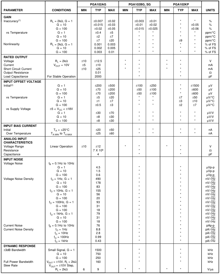
At +25°C, ±VCC = 15VDC unless otherwise specified.
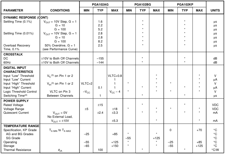
\* Specification same as AG grade. NOTES: (1) Gain inaccuracy is the percent error between the actual and ideal gain selected. It may be externally adjusted to zero for gains of 10 and 100. (2) Offset voltage can be adjusted for any one channel. Adjustment affects temperature drift by approximately ±0.3µV/°C for each 100µV of offset adjusted. (3) Voltage on the logic threshold control pin, VLTC, adjusts the threshold for “Low” and “High” logic levels. (4) Total time to settle equals switching time plus settling time of the newly selected gain.
The information provided herein is believed to be reliable; however, BURR-BROWN assumes no responsibility for inaccuracies or omissions. BURR-BROWN assumes no responsibility for the use of this information, and all use of such information shall be entirely at the user’s own risk. Prices and specifications are subject to change without notice. No patent rights or licenses to any of the circuits described herein are implied or granted to any third party. BURR-BROWN does not authorize or warrant any BURR-BROWN product for use in life support devices and/or systems.
Page 4
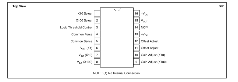
PIN CONFIGURATION
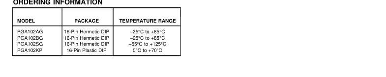
PACKAGE INFORMATION
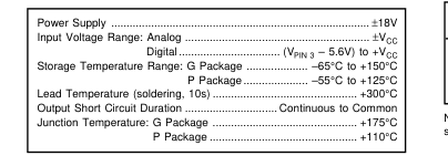
ABSOLUTE MAXIMUM RATINGS
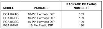
NOTE: (1) For detailed drawing and dimension table, please see end of data sheet, or Appendix D of Burr-Brown IC Data Book.
Page 5
TYPICAL PERFORMANCE CURVES
TA = +25°C, ±VCC = 15VDC unless otherwise noted.
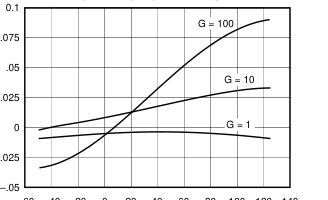
GAIN ERROR vs TEMPERATURE
–60 –40 –20 0 20 40 60 80 100 120 140
Temperature (°C)
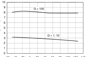
SETTLING TIME vs TEMPERATURE
–60 –40 –20 0 20 40 60 80 100 120 140
Temperature (°C)
–60 –40 –20 0 20 40 60 80 100 120 140
Temperature (°C)
NONLINEARITY vs TEMPERATURE
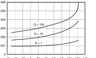
–60 –40 –20 0 20 40 60 80 100 120 140 Temperature (°C)
SMALL SIGNAL FREQUENCY RESPONSE
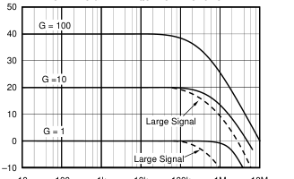
100 1k 10k
10
100k 1M 10M
Frequency (Hz)
SMALL SIGNAL STEP RESPONSE
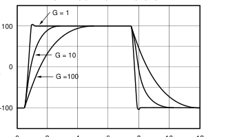
0 2 4 6 8 10 12
Time (µs)
Page 6
TYPICAL PERFORMANCE CURVES (CONT)
TA = +25°C, ±VCC = 15VDC unless otherwise noted.
LARGE SIGNAL STEP RESPONSE
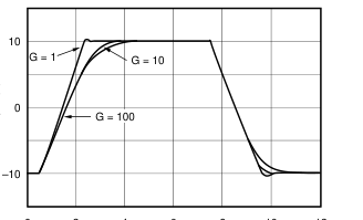
0 2 4 6 8 10 12
Time (µs)
INPUT VOLTAGE AND CURRENT NOISE vs FREQUENCY
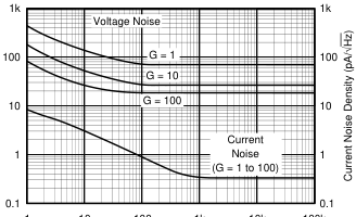
10 100 1k 10k 100k
1
Frequency (Hz)
POWER SUPPLY REJECTION vs FREQUENCY
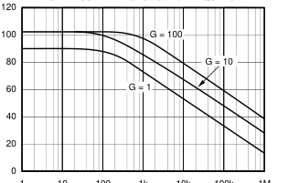
1M
1 10 100 1k 10k 100k
Frequency (Hz)
OVERLOAD RECOVERY vs INPUT OVERLOAD
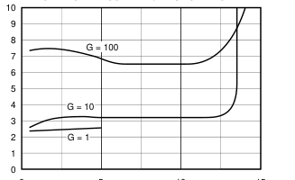
0
5
10
15
Input Overload Voltage (V)
INPUT CROSSTALK vs FREQUENCY
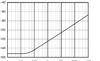
10 100 1k 10k 100k
1
1M
Frequency (Hz)
QUIESCENT CURRENT vs TEMPERATURE
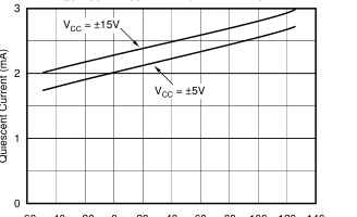
–60 –40 –20 0 20 40 60 80 100 120 140
Temperature (°C)
Page 7
APPLICATION INFORMATION
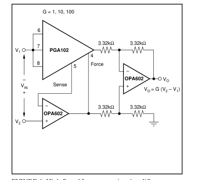
Figure 1 shows the basic connections required for operation of the PGA102. Power supplies should be bypassed with 0.1µF capacitors located close to the device pins. The inputs for each gain are independent and can be connected to three separate signal sources. Or, for many applications, the three inputs are connected in parallel to form a single input—see Figure 1. Only the input corresponding to the selected gain is active, operating as a non-inverting amplifier. The two inactive inputs behave as open circuits. The input bias current of the inactive inputs is negligible compared to that of the selected input.
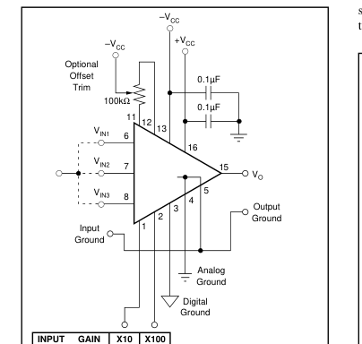
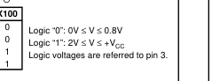
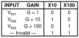
FIGURE 1. Basic Circuit Connections.
DIGITAL INPUTS
Gain is selected by the digital input pins, "X10" and “X100”. The threshold of these logic inputs is approximately 1.3V above the voltage on pin 3. For CMOS or TTL logic signals, connect pin 3 to logic ground. The logic inputs are not latched. Any change logic inputs immediately selects a new gain. Switching time is approximately 1µs. This does not include the time required for the analog output to settle to a new output value (see settling time specifications). Note that the two logic inputs allow four possible logic states—see Figure 1 for the logic table. A logic “1” on both inputs is an invalid code. This will not damage the device, but the analog output voltage will not be predictable while
this code is applied.
OFFSET ADJUSTMENT
The offset voltage of each of the three input stages is lasertrimmed. Many applications require no further adjustment. The optional trim circuit shown in Figure 1 can be used to adjust the offset voltage. This adjustment affects the offset of all three gain channels. Since each gain setting may require a different adjustment of the potentiometer, this requires a compromise. Often, offset voltage of the G = 100 channel is the most important, so adjustment can be optimized for this channel only. Alternatively, Figure 2 shows a CMOS switch used to select independent offset adjustment potentiometers for each of the three channels. Use these offset adjustment techniques only to null the offset
voltage of the PGA102. Do not null offset produced by the signal source or other system offsets or this will increase the temperature drift of the PGA102.
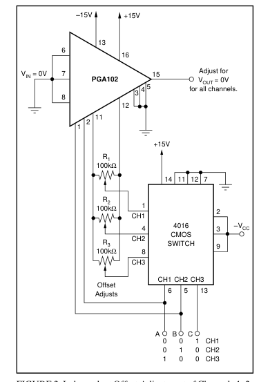
FIGURE 2. Independent Offset Adjustment of Channels 1, 2, and 3.
GAIN ADJUSTMENT
Gain of the PGA102 is accurately laser trimmed and usually requires no further adjustment. The optional circuit in Figure 3 allows independent gain adjustment of the G = 10 and G = 100 inputs.
Page 8
The gain of the G = 10 and G = 100 inputs can be changed
by adding external resistors to the internal feedback network
as shown in Figures 4 and 5. The internal gain-set resistors
are trimmed for precise ratios, not to exact values. The
internal resistor values are within approximately ±30% of
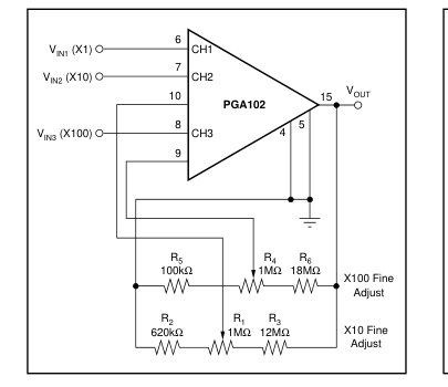
FIGURE 3. Optional Fine Gain Adjustment.
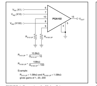
FIGURE 4. Connections for Higher Gains.
the nominal values shown on the front page diagram. This
makes the external resistor values in Figures 4 and 5 subject
to variation—especially for gains differing greatly from the
initial value.
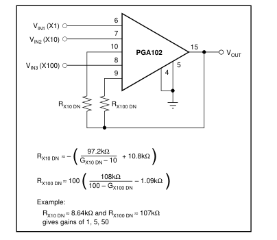
FIGURE 5. Connections for Lower Gains.