Download PDF
PFE3000-12-069RA BEL
Document overview
- PDF pages: 27
Technical content
Page 1

The PFE3000-12-069RA is a 3000 Watt AC/DC power-factorcorrected (PFC) and DC-DC power supply that converts standard AC mains power or high voltage DC bus voltages into a main output of 12 VDC for powering intermediate bus architectures (IBA) in high

performance and reliability servers, routers, and network switches.
The PFE3000-12-069RA meets international safety standards and displays the CE-Mark for the European Low Voltage Directive (LVD).
Best-in-class, Platinum efficiency Wide input voltage range: 90-300 VAC AC input with power factor correction DC input voltage range: 192-400 VDC
Parallel operation with active current sharing thru analog bus Full digital controls for improved performance High density design: 30.5 W/in3 Small form factor: 69 x 42 x 555 mm I2C communication interface with PMBus™ protocol for monitoring, control, and firmware update via bootloader Overtemperature, output overvoltage and overcurrent protection
2 Status LEDs: AC OK and DC OK with fault signaling Safety-approved to IEC/EN 60950-1 and UL/CSA 60950-1 2nd ed.
- Routers
- Switches

Page 2
2
ORDERING INFORMATION
PFE
3000
- 12 -
Product Family Power Level Dash V1 Output Dash
PFE Front-Ends
3000 W
12 V
1 Front to Rear 2.
OVERVIEW
069
R
A
Option Code Blank: Standard model
Width
Airflow
Input S366: Screw for Key-in
R: Reversed1 69 mm
A: AC
feature is installed.
The PFE3000-12-069RA is a fully DSP controlled, highly efficient front-end power supply. It incorporates resonant-soft-switching technology and interleaved power trains to reduce component stresses, providing increased system reliability and very high efficiency. With a wide input operating voltage range and minimal linear derating of output power with respect to ambient temperature, the PFE3000-12-069RA maximizes power availability in demanding server, switch, and router applications. The power supply is fan cooled and ideally suited for server integration with a matching airflow path. The PFC stage is digitally controlled using a state-of-the-art digital signal processing algorithm to guarantee best efficiency and
unity power factor over a wide operating range. The DC-DC stage uses soft switching resonant techniques in conjunction with synchronous rectification. An active OR-ing device on the output ensures no reverse load current and renders the supply ideally suited for operation in redundant power systems. The always-on +12V standby output provides power to external power distribution and management controllers. Its protection with an active OR-ing device provides for maximum reliability. Status information is provided with front-panel LEDs. In addition, the power supply can be monitored and controlled (i.e. fan speed setpoint) via I2C communication interface with PMBus protocol. It allows full monitoring of the supply, including input and output
voltage, current, power, and inside temperatures. The same I2C bus supports the bootloader to allow field update of the firmware in the DSP controllers. Cooling is managed by a fan, controlled by the DSP controller. The fan speed is adjusted automatically depending on the actual power demand and supply temperature and can be overridden through the I2C bus.
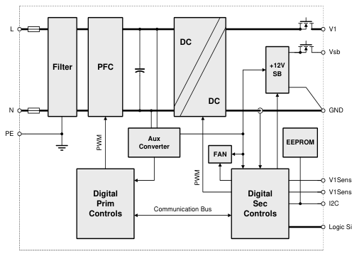
Logic Signals
Figure 1 - PFE3000-12-0069RA Block Diagram

1.
Page 3
3

INPUT

Vi AC Input Voltage Ranges
Normal operating (Vi min to Vi max)
90
300 VAC
Vinom DC DC Nominal input voltage
240
380 VDC
Vi DC DC Input voltage ranges
Normal operating (Vi min to Vi max)
192
400 VDC
Derated Input Voltage Vi red
See Figure 20 and Figure 33
90
180 VAC
Range Ii max Max Input Current
Vi > 200 VAC, >100 VAC
17 Arms
Ii p Inrush Current Limitation
Vi min to Vi max, 0 ° TNTC = 25°C (Figure 5)
50 Ap
Fi Input Frequency
47 50/60 63 Hz
PF Power Factor
Vi nom, 50Hz, > 0.3 I1 nom
0.96
W/VA
Turn-on Input Voltage2 Vi on
Ramping up
80
87 VAC
Turn-off Input Voltage2 Vi off
Ramping down
73
85 VAC
Vi nom, 0.1∙Ix nom, Vx nom, TA = 25°C
90.0 91.85
Vi nom, 0.2∙Ix nom, Vx nom, TA = 25°C
93.0 94.40
η Efficiency without Fan
%
Vi nom, 0.5∙Ix nom, Vx nom, TA = 25°C
94.5 94.95
Vi nom, Ix nom, Vx nom, TA = 25°C
93.0 93.75
After last AC zero point, V1 > 10.8 V,
Thold Hold-up Time
12
ms
VSB within regulation, Vi = 230 VAC, Px nom
2 The Front-End is provided with a minimum hysteresis of 3 V during turn-on and turn-off within the ranges
4.1 INPUT FUSE
Quick-acting 25 A input fuses (6.3 × 32 mm) in series with both the L- and N-line inside the power supply protect against severe defects. The fuses are not accessible from the outside and are therefore not serviceable parts.
4.2 INRUSH CURRENT
The AC-DC power supply exhibits an X capacitance of only 4.3μF, resulting in a low and short peak current, when the supply is connected to the mains. The internal bulk capacitor will be charged through an NTC which will limit the inrush current.
NOTE: Do not repeat plug-in / out operations below 90sec interval time at maximum input, high temperature condition, or else the internal in-rush current limiting device (NTC) may not sufficiently cool down and excessive inrush current or component failure(s) may result.

3.
Page 4
4
4.3 INPUT UNDER-VOLTAGE
If the RMS value of input voltage (either AC or DC) stays below the input undervoltage lockout threshold Vi on, the supply will be inhibited. Once the input voltage returns within the normal operating range, the supply will return to normal operation again.
4.4 POWER FACTOR CORRECTION
Power factor correction (PFC) (see Figure 4) is achieved by controlling the input current waveform synchronously with the input voltage. A fully digital controller is implemented giving outstanding PFC results over a wide input voltage and load ranges. The input current will follow the shape of the input voltage. If for instance the input voltage has a trapezoidal waveform, then the current will also show a trapezoidal waveform. At DC input voltage the PFC is still in operation, but the input current will be DC in this case.
4.5 EFFICIENCY
The high efficiency (see Figure 2) is achieved by using state-of-the-art silicon power devices in conjunction with soft-transition topologies minimizing switching losses and a full digital control scheme. Synchronous rectifiers on the output reduce the losses in the high current output path. The rpm of the fan is digitally controlled to keep all components at an optimal operating temperature regardless of the ambient temperature and load conditions. Figure 3 shows efficiency when input voltage is supplied from a high voltage DC source.
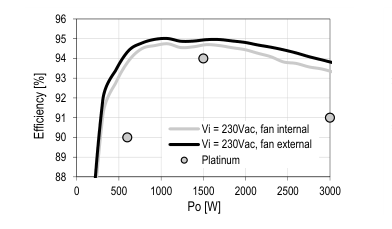
Figure 2 – AC Input Efficiency vs. Load current (ratio metric loading)
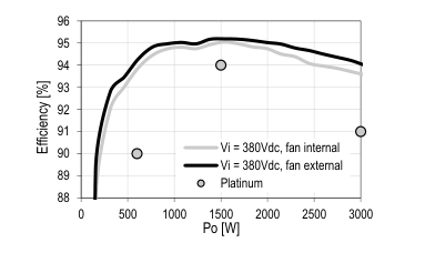
Figure 3 - DC Input Efficiency vs. load current (ratio metric loading)
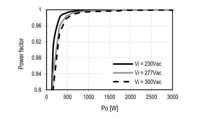
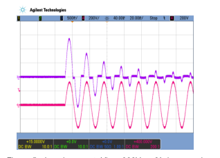
Figure 5 - Inrush current, Vin = 230Vac, 0°phase angle
Figure 4 - Power factor vs. Load current
CH4: Vin (200V/div), CH3: Iin (10A/div)

Page 5
5
OUTPUT
General Condition: TA = 0…45 °C unless otherwise noted.

dV1 tot Total Regulation
Vi min to Vi max,0 to 100% I1 nom,Ta min to Ta max
-1
+1 % V1 nom
P1 nom Nominal Output Power
V1 = 12.3 VDC, Vin < 180 VAC
1400
W
I1 nom Nominal Output Current
V1 = 12.3 VDC, Vin < 180 VAC
114
ADC
P1 nom Nominal Output Power
V1 = 12.3 VDC, Vin > 180 VAC
3000
W
I1 nom Nominal Output Current
V1 = 12.3 VDC, Vin > 180 VAC
244
ADC
V1 = 12.3 VDC, Vin > 180 VAC
IV1 ol Short time over load current Ta min to Ta max, maximum duration 20 ms
292 A
(See Section 5.2)
v1 pp Output Ripple Voltage
V1 nom, I1 nom, 20 MHz BW (See Section 5.1)
160 mVpp
dV1 Load Load Regulation
Vi = Vi nom, 0 - 100 % I1 nom
170
mV
dV1 Line Line Regulation
Vi =Vi min…Vi max
0
mV
Vi < 180 VAC, Ta < 45°C
120
127
Vi < 180 VAC, Ta = 55 °C 3)
92
99
IV1 ol lim Current limitation
ADC
Vi > 180 VAC, Ta < 45°C
248
274
Vi > 180 VAC, Ta = 55 °C 3)
186
212
dIshare Current Sharing
Deviation from I1 tot / N, I1 > 25% I1 nom
-5%
+5% A
ΔI1 = 50% I1 nom, I1 = 5 … 100% I1 nom, dI1/dt = 1A/μs, f ΔI1 = 0.05...10 kHz,
dVdyn Dynamic Load Regulation
-0.6
+0.6 V
Duty ΔI1 = 10...90%, recovery within 1% of V1 final steady state
Trec Recovery Time
0.5 ms
tAC V1 Start-up Time from AC
V1 = 10.8 VDC (see Figure 7)
3 sec
tV1 rise Rise Time
V1 = 10…90% V1 nom (see Figure 8)
2.5
ms
μF
CLoad Capacitive Loading
Ta = 25°C
30000
3 See Figure 20 for linear derating > 45°C
Stanby Output VSB
VSB nom Nominal Output Voltage
12
VDC
ISB nom, Tamb = 25°C
VSB set Output Setpoint Accuracy
-0.5
+0.5 %VSBnom
dVSB tot Total Regulation
Vi min to Vi max,ISB nom,Ta min to Ta max
-1
+1 %VSBnom
PSB nom Nominal Output Power
VSB = 12 VDC
60
W
ISB nom Nominal Output Current
VSB = 12 VDC
5
ADC
VSB pp Output Ripple Voltage
VSB nom, ISB nom, 20 MHz BW (See Section 5.1)
300 mVpp
dVSB Droop
0 - 100 % ISB nom
400
mV
IVSB lim Current Limitation
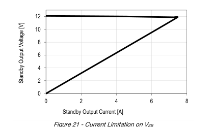
6
9 ADC
ΔISB = 50% ISB nom, ISB = 5 … 100% ISB nom, dIo/dt = 1A/μs, f ΔI1 = 0.05...10kHz, Duty ΔI1 =
dVSBdyn Dynamic Load Regulation
-0.6
+0.6 VSBnom
10...90%, recovery within 1% of VSB final steady state
Trec Recovery Time
0.5 ms
tAC VSB Start-up Time from AC
VSB = 90% VSB nom (see Figure 7)
3 sec
tVSB rise Rise Time
VSB = 10…90% VSB nom (see Figure 9))
10
ms
μF
CLoad Capacitive Loading
Tamb = 25°C
3000

5.
Page 6
6
5.1 OUTPUT VOLTAGE RIPPLE
The internal output capacitance at the power supply output (behind OR-ing element) is minimized to prevent disturbances during hot plug. In order to provide low output ripple voltage in the application, external capacitors should be added close to the power supply output. The setup of Figure 6 has been used to evaluate suitable capacitor types. The capacitor combinations of Table 1 and Table 2 should be used to reduce the output ripple voltage. The ripple voltage is measured with 20 MHz BWL, close to the external capacitors.
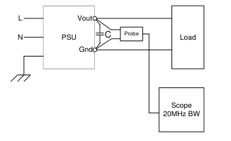
Figure 6 - Output Ripple Test Setup
NOTE: Care must be taken when using ceramic capacitors with a total capacitance of 1 µF to 50 µF on output V1, due to their high quality factor the output ripple voltage may be increased in certain frequency ranges due to resonance effects.
External Capacitor V1
dV1max Unit
2Pcs 47µF/16V/X5R/1210
160 mVpp
1Pcs 1000µF/16V/Low ESR
160 mVpp
Aluminum/ø10x20 1Pcs 270µF/16V/Conductive
160 mVpp
Polymer/ø8x12 2Pcs 47µF/16V/X5R/1210 plus 1Pcs 270µF Conductive Polymer OR 90
mVpp
1Pcs 1000µF Low ESR AlCap
Table 1 - Suitable Capacitors for V1
External capacitor VSB
dVSBmax Unit
1Pcs 10µF/16 V/X7R/1206
300 mVpp
Table 2 - Suitable Capacitors for VSB
The output ripple voltage on VSB is influenced by the main output V1. Evaluating VSB output ripple must be done when maximum load is applied to V1.
5.2 SHORT TIME OVERLOAD
The main output has the capability to allow load current up to 20% above the nominal output current rating for a maximum duration of 20 ms. This allows the system to consume extended power for short time dynamic processes.
5.3 OUTPUT ISOLATION
Main and standby output and all signals are isolated from the chassis and protective earth connection, although the applied voltage must not exceed 100 Vpeak to prevent any damage of the supply. Internal to the supply the main output ground, standby output ground and signal ground are interconnected through 10Ω resistors to prevent any circulating current within the supply. In order to prevent any potential difference in outputs or signals within the application these 3 grounds must be directly interconnected at system level. See also section 14 for pins to be interconnected.

Page 7
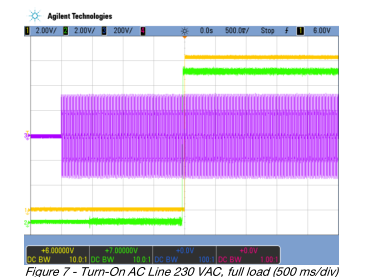
CH1: V1 (2 V/div); CH2: VSB (2 V/div); CH3: Vin (200 V/div)
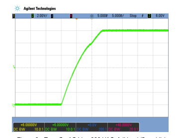
Figure 9 - Turn-On AC Line 230 VAC, full load (5 ms/div)
CH2: VSB (2 V/div)
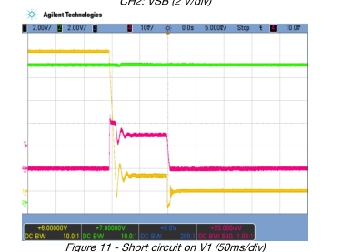
CH1: V1 (2V/div) CH2: VSB (2V/div) CH4: I1 (200A/div)

7
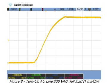
CH1: V1 (2 V/div)
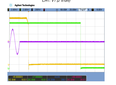
Figure 10 - Turn-Off AC Line 230 VAC, full load (20 ms/div) CH1: V1 (2 V/div); CH2: VSB (2 V/div); CH3: Vin (200 V/div)
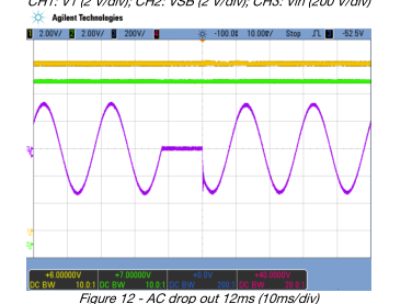
CH1: V1 (2V/div) CH2: VSB (2V/div) CH3: Vin (200V/div)
Page 8
8
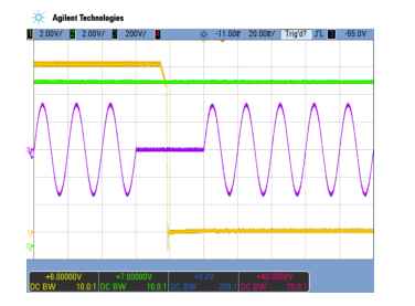
Figure 13 - AC drop out 40 ms, full load (20 ms/div) CH1: V1 (2 V/div); CH2: VSB (2 V/div); CH3: Vin (200 V/div)
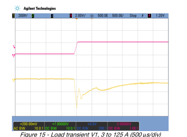
CH1: V1 (200 mV/div); CH4: I1 (100 A/div)
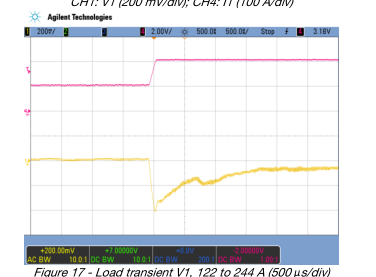
CH1: V1 (200 mV/div); CH4: I1 (100 A/div)

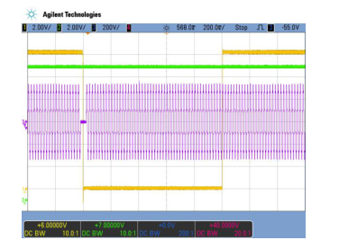
Figure 14 - AC drop out 40 ms, full load (200 ms/div),V1 restart after 1 sec CH1: V1 (5 V/div); CH2: VSB (2 V/div);
CH3: I1 (200 V/div)
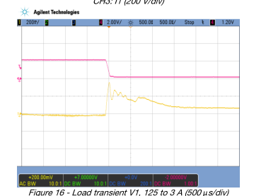
CH1: V1 (200 mV/div); CH4: I1 (100 A/div)
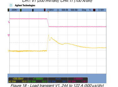
CH1: V1 (200 mV/div); CH4: I1 (100 A/div)
Page 9
9
PROTECTION
PARAMETER
DESCRIPTION / CONDITION
MIN NOM MAX UNIT
F Input Fuses (L+N)
Not user accessible, quick-acting (F)
25
A
V1 OV OV Threshold V1
13.6 14.2 14.8 VDC
tOV V1 OV Latch Off Time V1
1 ms
VSB OV OV Threshold VSB
13.3 13.9 14.5 VDC
tOV VSB OV Latch Off Time VSB
1 ms
Vi < 180 VAC, Ta < 45°C
120
127
Vi < 180 VAC, Ta = 55 °C 4
92
99
IV1 lim Current limitation
A
Vi > 180 VAC, Ta < 45°C
248
274
Vi > 180 VAC, Ta = 55 °C 4
186
212
tV1 lim Current limit blanking time
Time to latch off when in over current
20 22 24 ms
Current limit during short time IV1 ol lim
Maximum duration 20 ms
292 300 308 A
overload V1
350 5
IV1 SC Max Short Circuit Current V1
V1 < 3 V
A
tV1 SC off Short circuit latch off time
Time to latch off when in short circuit
10
ms
IVSB lim Current limitation VSB
6
9 A
tVSB lim Current limit blanking time
Time to hit hiccup when in over current
1 ms
Inlet Ambient Temperature
60
PFC Primary Heatsink Temperature
80
TSD Over temperature on critical points
°C
Secondary Sync Mosfet Temperature
115
Secondary OR-ing Mosfet Temperature
125
4 See Figure 20 for linear derating > 45° 5 Limit set don’t include effects of main output capacitive discharge.
6.
6.1 AUTOMATIC RETRY
For all fault conditions except current limitation on Standby output, the supply will shut down for 10sec and restart automatically. The supply will auto-restart from a fault up to 5 times, after that it will latch off. The latch and restart counter can be cleared by recycling the input voltage or the PSON_L input. A failure on the Standby output will shut down both Main and Standby outputs. A failure on the Main output will shut down only the Main output, while Standby continues to operate.
6.2 OVERVOLTAGE PROTECTION
The PFE front-ends provide a fixed threshold overvoltage (OV) protection implemented with a HW comparator. Once an OV condition has been triggered, the supply will shut down and latch the fault condition.
6.3 UNDERVOLTAGE DETECTION
Both main and standby outputs are monitored. LED and PWOK_L pin signal if the output voltage exceeds ±7% of its nominal voltage. Output undervoltage protection is provided on both outputs. When either V1 or VSB falls below 93% of its nominal voltage, the output is inhibited.

Page 10
10
6.4 CURRENT LIMITATION
MAIN OUTPUT
Two different over current protection features are implemented on the main output. A static over current protection will shut down the output, if the output current does exceed IV1 lim for more than 20ms. If the output current is increased slowly this protection will shut down the supply. The main output current limitation level IV1 lim will decrease if the ambient (inlet) temperature increases beyond 45 °C (see Figure 20). Note that the actual current limitation on V1 will kick in at a current level approximately 20 A higher than what is shown in Figure 20 (see also section 9 for additional information). The 2nd protection is a substantially rectangular output characteristic controlled by a software feedback loop. This protects the
power supply and system during the 20ms blanking time of the static over current protection. If the output current is rising fast and reaches IV1 ol lim, the supply will immediately reduce its output voltage to prevent the output current from exceeding IV1 ol lim. When the output current is reduced below IV1 ol lim, the output voltage will return to its nominal value.
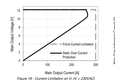
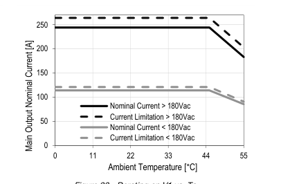
Figure 20 - Derating on V1 vs. Ta
STANDBY OUTPUT
On the standby output a hiccup type over current protection is implemented. This protection will shut down the standby output immediately when standby current reaches or exceeds IVSB lim. After an off-time of 1s the output automatically tries to restart. If the overload condition is removed the output voltage will reach again its nominal value. At continuous overload condition the output will repeatedly trying to restart with 1s intervals.

Page 11
11
MONITORING
DESCRIPTION / CONDITION
PARAMETER
MIN NOM MAX UNIT
Vi min ≤ Vi ≤ Vi max
Vi mon Input RMS Voltage
-2.5
+2.5 %
Ii > 4 Arms
-5
+5 %
Ii mon Input RMS Current
Ii ≤ 4 Arms
-0.2
+0.2 Arms
Pi > 700 W
-5
+5 %
Pi mon True Input Power
Pi ≤ 700 W
-35
+35 W
Pi > 700 W
-5
+5 %
Ei mon Total Input Energy
Pi ≤ 700 W
-35
+35 Wh
V1 mon V1 Voltage
-2
+2 %
I1 > 30 A
-2
+2 %
I1 mon V1 Current
I1 ≤ 30 A
-0.6
+0.6 A
Po > 200 W
-5
+5 %
Po nom Total Output Power
Po ≤ 200 W
-10
+10 W
Po > 200 W
-5
+5 %
Eo mon Total Output Energy
Po ≤ 200 W
-10
+10 Wh
VSB mon Standby Voltage
-2
+2 %
ISB ≤ ISB nom
ISB mon Standby Current
-0.3
+0.3 A
7.

Page 12
12
SIGNALING AND CONTROL
8.1 ELECTRICAL CHARACTERISTICS
PARAMETER
DESCRIPTION / CONDITION
MIN NOM MAX UNIT
PSKILL / PSON_L inputs
VIL
Input low level voltage
-0.2
0.8 V
VIH
Input high level voltage
2.0
3.6 V
IIL, H
Maximum input sink or source current
0
1 mA
kΩ
RpuPSKILL
Internal pull up resistor on PSKILL
10
kΩ
RpuPSON_L
Internal pull up resistor on PSON_L
10
PWOK_L output
VOL
Output low level voltage
Isink < 4 mA
-0.2
0.4 V
VpuPWOK_L
External pull up voltage
12 V
Recommended external pull up resistor on
kΩ
RpuPWOK_L
10
PWOK_L at VpuPWOK_L = 3.3 V
Low level output
All outputs are turned on and within regulation

VpuINOK_L
External pull up voltage
12 V
Recommended external pull up resistor on
kΩ
RpuINOK_L
10
INOK_L at VpuINOK_L= 3.3 V
Low level output
Input voltage is within range for PSU to operate

VpuSMB_ALERT_L
External pull up voltage
12 V
Recommended external pull up resistor on
kΩ
RpuSMB_ALERT_L
10
SMB_ALERT_L at VpuSMB_ALERT_L= 3.3 V
Low level output
PSU in warning or failure condition
High level output
PSU is ok
8.
8.2 INTERFACING WITH SIGNALS
A 15V zener diode is added on all signal pins versus signal ground SGND to protect internal circuits from negative and high positive voltage. Signal pins of several supplies running in parallel can be interconnected directly. A supply having no input power will not affect the signals of the paralleled supplies. ISHARE pins must be interconnected without any additional components. This in-/output also has a 15 V zener diode as a protection device and is disconnected from internal circuits when the power supply is switched off.
8.3 FRONT LEDs
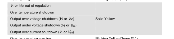
The front-end has 2 front LEDs showing the status of the supply. LED number one is green and indicates AC power is on or off, while LED number two is bi-colored: green and yellow, and indicates DC power presence or fault situations. For the position of the LEDs see Table 3 listing the different LED status.

Page 13
OPERATING CONDITION
AC LED
AC Line within range
AC Line UV condition
DC LED \*
Normal Operation
PSON_L High
13
LED SIGNALING
Solid Green
Off
Solid Green
Blinking Yellow (1:1)
Over temperature warning
Blinking Yellow/Green (2:1)
Minor fan regulation error (>5%, <15%)
Blinking Yellow/Green (1:1)
\* The order of the criteria in the table corresponds to the testing precedence in the controller.
Table 3 - LED Status
8.4 PRESENT_L
The PRESENT_L is normally a trailing pin within the connector and will contact only once all other connector contacts are closed. This active-low pin is used to indicate to a power distribution unit controller that a supply is plugged in. The maximum sink current on PRESENT_L pin should not exceed 10 mA.
PFE
PDU
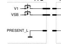
Figure 22 - PRESENT_L signal pin
8.5 PSKILL INPUT
The PSKILL input is an active-low and normally a trailing pin in the connector and is used to disconnect the main output as soon as the power supply is being plugged out. This pin should be connected to SGND in the power distribution unit. The standby output will remain on regardless of the PSKILL input state.
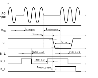
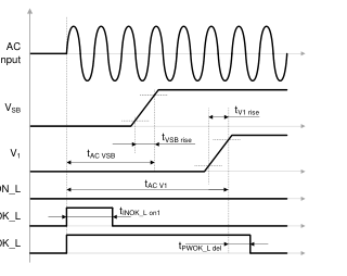
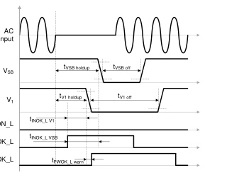
8.6 AC TURN-ON / DROP-OUTS / INOK_L
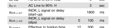
The power supply will automatically turn-on when connected to the AC line under the condition that the PSON_L signal is pulled low and the AC line is within range. The INOK_L is an open collector output that requires an external pull-up to a maximum of 12V indicating whether the input is within the range the power supply can use and turn on. The INOK_L signal is active-low. The timing diagram is shown in Figure 23 and referenced in Table 4.

Page 14
14
OPERATING CONDITION
MIN MAX UNIT
tAC VSB AC Line to 90% VVSB
3 sec
tV1 holdup Effective V1 holdup time
12 300 ms
tVSB holdup Effective VSB holdup time
40 300 ms
tINOK_L V1 INOK_L to V1 holdup
7 ms
tINOK_L VSB INOK_L to VSB holdup
27 ms
tV1 off Minimum V1 off time
1000 1200 ms
tVSB off Minimum VSB off time
1000 1200 ms
tV1dropout Minimum V1 dropout time
12 ms
tVSBdropout Minimum VSB dropout time 40
ms
Table 4 - AC Turn-on / Dip Timing
PSON_L
INOK_L
PWOK_L
Figure 24 - AC short dips
8.7 PSON_L INPUT
PSON_L
INOK_L
PWOK_L
Figure 23 - AC turn-on timing
PSON_L
INOK_L
PWOK_L
Figure 25 - AC long dips
The PSON_L is an internally pulled-up (3.3 V) input signal to enable / disable the main output V1 of the front-end. This active-low pin is also used to clear any latched fault condition. The timing diagram is given in Figure 26 and the parameters in Table 5.
OPERATING CONDITION
MIN MAX UNIT
tPSON_L V1on PSON_L to V1 delay (on)
190 220 ms
tPSON_L V1off PSON_L to V1 delay (off)
0 100 ms
Table 5 - PSON_L timing
8.8 PWOK_L SIGNAL
The PWOK_L is an open collector output that requires an external pull-up to a maximum of 12 V indicating whether both VSB and V1 outputs are within regulation. This pin is active-low. The timing diagram is shown in Figure 26 and referenced in Table 6.

Page 15
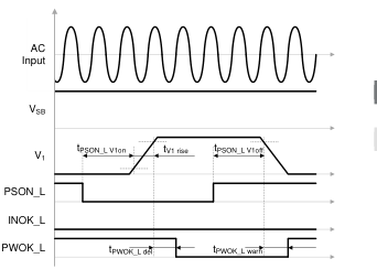
Figure 26 - PSON_L turn-on/off timing
8.9 CURRENT SHARE
15
OPERATING CONDITION
MIN MAX UNIT
tPWOK_L del V1 to PWOK_L delay (on)
250 350 ms
tPWOK_L warn V1 to PWOK_L delay (off)
0 5 ms
Table 6 - PWOK_L timing
The PFE front-ends have an active current share scheme implemented for V1. All the ISHARE current share pins need to be interconnected in order to activate the sharing function. If a supply has an internal fault or is not turned on, it will disconnect its ISHARE pin from the share bus. This will prevent dragging the output down (or up) in such cases. The current share function uses an analog bus. The controller implements a Master/Slave current share function. The power supply providing the largest current among the group is automatically the Master. The other supplies will operate as Slaves and increase their output current to a value close to the Master by slightly increasing their output voltage. The voltage increase
is limited to +250 mV. The standby output uses a passive current share method (droop output voltage characteristic).
Maximum available power on main
No of paralleled PSUs
12 V without redundancy
1
3000 W
2
5850 W
3
8700 W
4
11550 W
5
14400 W
6
17250 W
Maximum available power on main Maximum available power 12 V with n+1 redundancy
on standby output
-
60 W
3000 W
60 W
5850 W
60 W
8700 W
60 W
11550 W
60 W
14400 W
60 W
Table 7 - Power available when PSU in redundant operation
8.10
SENSE INPUTS
Main output has sense lines implemented to compensate for voltage drop on load wires. The maximum allowed voltage drop is 200 mV on the positive rail and 100 mV on the PGND rail. With open sense inputs the main output voltage will rise by 250 mV. Therefore if not used, these inputs should be connected to the power output and PGND close to the power supply connector. The sense inputs are protected against short circuit. In this case the power supply will shut down.
8.11 I2C / PMBus COMMUNICATION
The interface driver in the PFE supply is referenced to the SGND. The PFE supply is a communication slave device only; it never initiates messages on the I2C bus by itself. The communication bus voltage and timing is defined in Table 8 and further characterized through:

Page 16
16
| 3.3V RX 100kΩ TX PFE | 3.3V |
- There are 100 kΩ internal pull-up resistors
- The SDA/SCL IOs must be pull-up externally to 3.3 ± 0.3 V
Rpull-up
- Pull-up resistor should be 2 – 5 kΩ to ensure SMBUS
SDA/SCL
compliant signal rise times
- I2C clock speed up to 100 kbps
- Clock stretching limited to 1 ms
- SCL low time-out of >25 ms with recovery within 10 ms
- Recognizes any time Start/Stop bus conditions
Figure 27 - Physical layer of communication interface
The SMB_ALERT_L signal indicates that the power supply is experiencing a problem that the system agent should investigate. This is a logical OR of the Shutdown and Warning events. Communication to the DSP or the EEPROM will be possible as long as the input AC (DC) voltage is provided. If no AC (DC) is present, communication to the unit is possible as long as it is connected to a live VSB output (provided e.g. by the redundant unit). If only V1 is provided, communication is not possible.
PARAMETER
DESCRIPTION
ViL
Input low voltage
ViH
Input high voltage
Vhys
Input hysteresis
VoL
Output low voltage
tr
Rise time for SDA and SCL
Output fall time ViHmin ViLmax
tof
Ii
Input current SCL/SDA
Ci
Capacitance for each SCL/SDA
fSCL
SCL clock frequency
Rpu
External pull-up resistor
tHDSTA
Hold time (repeated) START
tLOW
Low period of the SCL clock
tHIGH
High period of the SCL clock
tSUSTA
Setup time for a repeated START
tHDDAT
Data hold time
tSUDAT
Data setup time
tSUSTO
Setup time for STOP condition
tBUF
Bus free time between STOP and START
EEPROM_WP
ViL
Input low voltage
ViH
Input high voltage
Ii
Input sink or source current
Rpu
Internal pull-up resistor to 3.3V
CONDITION
MIN
MAX UNIT
-0.2
0.4
V
2.1
3.6
V
0.15
V
4 mA sink current
0 0.4
V
20+0.1Cb\*
300
ns
10 pF < Cb\* < 400 pF
20+0.1Cb\*
250
ns
μA
0.1 VDD < Vi < 0.9 VDD
-10
10
10 pF
0 100 kHz
Ω
fSCL ≤ 100 kHz
1000 ns / Cb\*
fSCL ≤ 100 kHz
μs
4.0
fSCL ≤ 100 kHz
μs
4.7
fSCL ≤ 100 kHz
μs
4.0
fSCL ≤ 100 kHz
μs
4.7
fSCL ≤ 100 kHz
μs
0 3.45
fSCL ≤ 100 kHz
250
ns
fSCL ≤ 100 kHz
μs
4.0
fSCL ≤ 100 kHz
μs
4.7
-0.2
0.4
V
2.1
3.6
V
-1
1 mA
Ω
10k
\* Cb = Capacitance of bus line in pF, typically in the range of 10…400 pF
Table 8 - I2C / SMBus Specification

Page 17
17
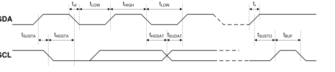
Figure 28 - I2C / SMBus Timing
8.12
ADDRESS
The supply supports PMBus communication protocol, address for PMBus communication is at fixed to 0x20. The EEPROM is at fixed address = 0xA0.
8.13
CONTROLLER AND EEPROM ACCESS
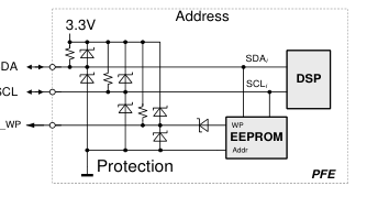
The controller and the EEPROM in the power supply share the same I2C bus physical layer (see Figure 29). In order to write to the EEPROM, the write protection needs to be disabled by setting EEPROM_WP input correctly. If EEPROM_WP is High, write is not allowed to the EEPROM and if Low, write is allowed. The EEPROM provides 2k bytes of user memory. None of the bytes are used for the operation of the power supply.
EEPROM_WP
Figure 29 - I2C Bus to DSP and EEPROM
8.14
EEPROM PROTOCOL
The EEPROM follows the industry communication protocols used for this type of device. Even though page write / read commands are defined, it is recommended to use the single byte write / read commands.
WRITE
The write command follows the SMBus 1.1 Write Byte protocol. After the device address with the write bit cleared a first byte with the data address to write to is sent followed by the data byte and the STOP condition. A new START condition on the bus should only occur after 5ms of the last STOP condition to allow the EEPROM to write the data into its memory.
S Address W A
Data Address A Data A P
READ
The read command follows the SMBus 1.1 Read Byte protocol. After the device address with the write bit cleared the data address byte is sent followed by a repeated start, the device address and the read bit set. The EEPROM will respond with the data byte at the specified location.

Page 18
18
S Address W A
Data Address A
S Address R A
Data nA P
8.15
PMBus™ PROTOCOL
The Power Management Bus (PMBus™) is an open standard protocol that defines means of communicating with power
conversion and other devices. For more information, please see the System Management Interface Forum web site at:
www.powerSIG.org.
PMBus™ command codes are not register addresses. They describe a specific command to be executed.
PFE3000-12-069RA supply supports the following basic command structures:
- Clock stretching limited to 1 ms
- SCL low time-out of >25 ms with recovery within 10 ms
- Recognized any time Start/Stop bus conditions
WRITE
The write protocol is the SMBus 1.1 Write Byte/Word protocol. Note that the write protocol may end after the command byte
or after the first data byte (Byte command) or then after sending 2 data bytes (Word command).
S Address W A
Command A
Data Low Byte1) A Data High Byte1) A
P
1) Optional
In addition, Block write commands are supported with a total maximum length of 255 bytes. See PFE3000-12-069RA PMBus
Communication Manual BCA.00070 for further information.
S Address W A
Command A Byte Count A
Byte 1 A
Byte N A P
READ
The read protocol is the SMBus 1.1 Read Byte/Word protocol. Note that the read protocol may request a single byte or word.
S Address W A
Command A
Data High Byte1) nA P
S Address R A Data (Low) Byte A
1) Optional
In addition, Block read commands are supported with a total maximum length of 255 bytes. See PFE3000-12-069RA PMBus
Communication Manual BCA.00070 for further information.
S Address W A
Command A S Address R A
Byte Count A
Byte 1 A Byte N nA P

Page 19
19
8.16
GRAPHICAL USER INTERFACE
Bel Power Solutions I2C Utility provides a Windows® Vista/Win7/8 compatible graphical user interface allowing the programming and monitoring of the PFE3000-12-069RA Front-End. The utility can be downloaded on www.belpowersolutions.com and supports the PMBus™ protocol. The GUI allows automatic discovery of the units connected to the communication bus and will show them in the navigation tree. In the monitoring view the power supply can be controlled and monitored. If the GUI is used in conjunction with the PFE3000-12-069RA Evaluation Kit it is also possible to control the PSON_L pin(s) of the power supply.
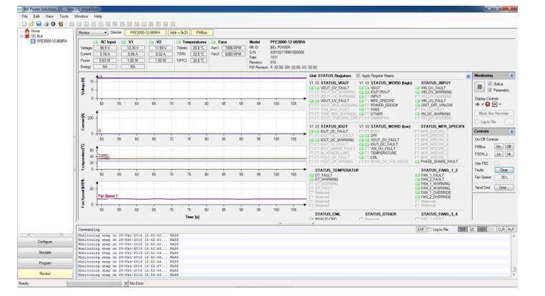
Figure 30 - Monitoring dialog of the I2C Utility
9.
TEMPERATURE AND FAN CONTROL
To achieve best cooling results sufficient airflow through the supply must be ensured. Do not block or obstruct the airflow at the rear of the supply by placing large objects directly at the output connector. The PFE3000-12-069RA is provided with a reverse airflow, which means the air enters through the front of the supply and leaves at the rear. PFE supplies have been designed for horizontal operation. The fan inside of the supply is controlled by a microprocessor. The rpm of the fan is adjusted to ensure optimal supply cooling and is a function of output power and the inlet temperature.


Page 20
20
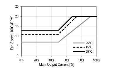
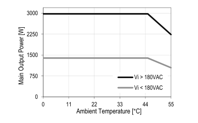
Figure 32 - Fan speed vs. main output load for
Figure 33 - Thermal derating for PFE3000-12-069RA 10.
ELECTROMAGNETIC COMPATIBILITY
10.1
IMMUNITY
NOTE: Most of the immunity requirements are derived from EN 55024:1998/A2:2003.
PARAMETER
DESCRIPTION / CONDITION
CRITERION
IEC / EN 61000-4-2, ±8 kV, 25+25 discharges per test point
ESD Contact Discharge
A
(metallic case, LEDs, connector body) IEC / EN 61000-4-2, ±15 kV, 25+25 discharges per test point
ESD Air Discharge
A
(non-metallic user accessible surfaces) IEC / EN 61000-4-3, 10 V/m, 1 kHz/80% Amplitude Modulation,
Radiated Electromagnetic Field
A
1 µs Pulse Modulation, 10 kHz…2 GHz IEC / EN 61000-4-4, level 3
Burst
AC port ±2 kV, 1 minute
A
DC port ±1 kV, 1 minute IEC / EN 61000-4-5
Surge
Line to earth: level 3, ±2 kV
A
Line to line: level 2, ±1 kV IEC/EN 61000-4-6, Level 3, 10 Vrms, CW, 0.1 … 80 MHz
RF Conducted Immunity
A
IEC/EN 61000-4-11 1: Vi 230Volts, 100% Load, Dip 100%, Duration 12ms
A
Voltage Dips and Interruptions
2: Vi 230Volts, 100% Load, Dip 100%, Duration < 150 ms
V1: B, VSB: A
- Vi 230Volts, 100% Load, Dip 100%, Duration > 150 ms
B
10.2
EMISSION
PARAMETER
DESCRIPTION / CONDITION
CRITERION
EN55022 / CISPR 22: 0.15 … 30 MHz, QP and AVG
Conducted Emission
Class A
EN55022 / CISPR 22: 30 MHz … 1 GHz, QP
Radiated Emission
Class A
IEC61000-3-2, Vin = 115/230 VAC, 50 Hz, 100% Load
Harmonic Emissions
Class A
Sound power statistical declaration (ISO 9296, ISO 7779, IS9295)
Acoustical Noise
60 dBA
@ 50% load IEC / EN 61000-3-3, dmax < 3.3%
AC Flicker
PASS

Page 21
21
SAFETY / APPROVALS
Maximum electric strength testing is performed in the factory according to IEC/EN 60950, and UL 60950. Input-to-output electric strength tests should not be repeated in the field. Bel Power Solutions will not honor any warranty claims resulting from electric strength field tests. 12.
PARAMETER
DESCRIPTION / CONDITION
MIN NOM MAX UNIT
Approved to the latest edition of the following standards: • IEC60950-1 2nd edition (CB)
- EN60950-1 2nd Edition (Nemko)
- UL/CSA0950-1 2nd Edition (cCSAus)
Agency Approvals
- CNS14336-1, CNS13438 (BSMI)
- EAC, TR-CU (Russia)
- BIS, (India) Input (L/N) to case (PE)
Basic
Isolation Strength
Input (L/N) to output
Reinforced
Output to case (PE)
Functional
Primary (L/N) to protective earth (PE)
dC Creepage / Clearance
Primary to secondary Input to case
2121
Electrical Strength Test
VDC
Input to output (tested by manufacturer only)
4242
ENVIRONMENTAL13.
PARAMETER
DESCRIPTION / CONDITION
MIN NOM MAX UNIT
Vi min to Vi max, I1 nom, ISB nom at 4000m
0
+35 °C
TA Ambient Temperature
Vi min to Vi max, I1 nom, ISB nom at 1800m
0
+45 °C
TAext Extended Temp. Range
Derated output (see Figure 20 and Figure 33) at 1800m
+45
+55 °C
TS Storage Temperature
Non-operational
-40
+70 °C
Altitude
Operational, above Sea Level (see derating)
-
4000 m
Na Audible Noise
Vi nom, 50% Io nom, TA = 25°C
60
dBA
Cooling
System Back Pressure
0.5 in-H20
MECHANICAL
PARAMETER
DESCRIPTION / CONDITION
MIN NOM MAX UNIT
Width
69
mm
Dimensions
Heigth
42
mm
Depth
555
mm
m Weight
2.60
kg
NOTE: A 3D step file of the power supply casing is available on request.
11.

Page 22
22
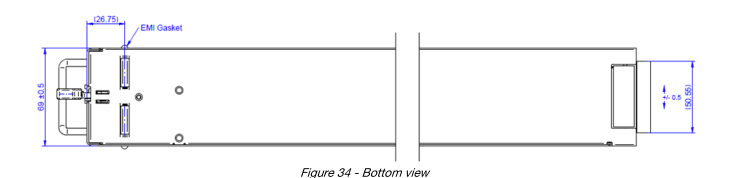
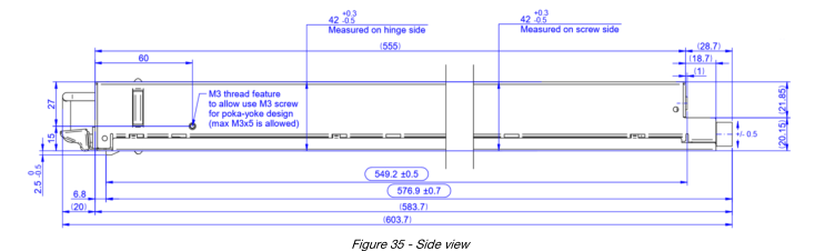
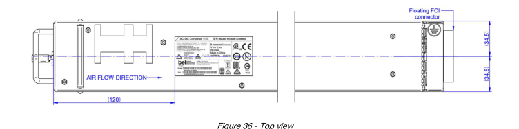
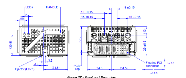
Figure 37 - Front and Rear view

Page 23
23
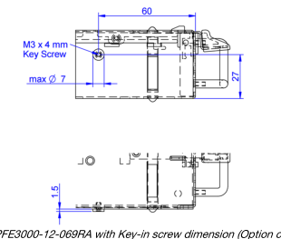
Figure 38 - PFE3000-12-069RA with Key-in screw dimension (Option code S366)
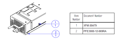
Figure 39 - PFE3000-12-069RA with Key-in screw (Option code S366)
14.
CONNECTORS
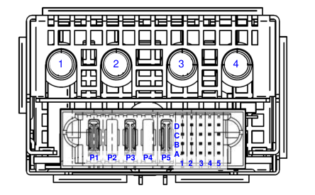
Unit: FCI Connectors P/N 51939-768LF Note: A1 and A2 are Trailing Pin (short pins) Counterpart: FCI Connectors P/N 51915-401LF For Main Output Pins, see section 15

Page 24
24
PIN
NAME
DESCRIPTION
Output
3,4
V1
+12 VDC main output
1,2
PGND
+12 VDC main output ground
Input Pins
P1
LIVE
AC Live Pin
P2
N.C
No metal pin connection
P3
NEUTRAL
AC Neutral Pin
P4
N.C.
No metal pin connection
P5
P.E.
Protective Earth Pin
Control Pins
A1
PSKILL
Power supply kill (trailing pin): active-high
B1
PWOK_L
Power OK signal output: active-low
C1
INOK_L
Input OK signal: active-low
D1
PSON_L
Power supply on input: active-low
A2
PRESENT_L
Power supply present (trailing pin): active-low
B2
SGND
Signal ground\* (return)
C2
SGND
Signal ground\* (return)
D2
SGND
Signal ground\* (return)
I2C clock signal line
A3
SCL
I2C data signal line
B3
SDA
C3
SMB_ALERT_L
SMB Alert signal output: active-low
D3
ISHARE
V1 Current share bus
A4
EEPROM_WP
EEPROM write protect
B4
RESERVED
Reserved
C4
V1_SENSE_R
Main output negative sense
D4
V1_SENSE
Main output positive sense
A5
VSB
Standby positive output
B5
VSB
Standby positive output
C5
VSB_GND
Standby Ground\*
D5
VSB_GND
Standby Ground\*
\* These pins should be connected to PGND on the system. See Section 8 for pull up resistor settings of signal pins. All signal pins are referred to SGND
Figure 40 – Pin assignment

Page 25
25
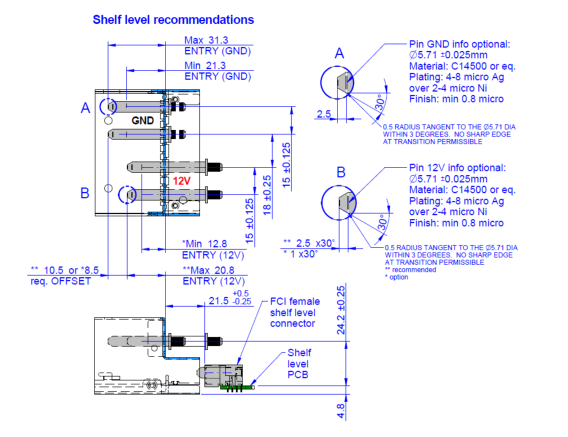
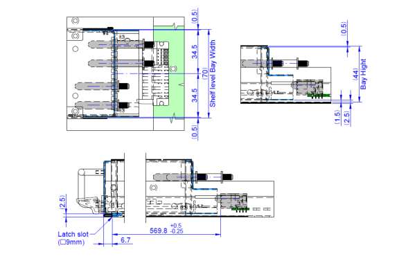
SHELF LEVEL CONFIGURATION (PROVISIONAL)
The recommended pin configuration below is based on company’s own Shelf design and provided here as reference. Customer pin lengths within the range indicated is acceptable.

15.
Page 26
26
ACCESSORIES
ITEM
DESCRIPTION
ORDERING PN
SOURCE
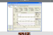
I2C Utility Windows Vista/7/8 compatible GUI to program, control and
N/A
www.belpowersolutions.com
monitor PFE Front-Ends (and other I2C units)

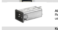
C20F.0011
AC Can Filter Recommended AC can filter used on system side.
20GENG3E-R
Key-in Screw
XFM.00479
Screw for PSU Orientation.
16.

Schurter Inc.
Delta Electronics
Focus Metal
Page 27
27
REVISION HISTORY
PSU PRODUCT
REV
DESCRIPTION
DATE AUTHOR
VERSION V001
AA Initial Release of Datasheet.
V004
11-27-2013
GS
V007
▪ Handle position and size has changed to a diagonal format to allow better handling/grip. ▪ +12VSB turn-on delay is changed from 2 seconds to 3 seconds. AB
V008
10-22-2014
GS
Main output will only turn on (if enabled by PSKILL and PSON) once +12VSB is in regulation. ▪ Datasheet format was changed to Bel Power Solution. ▪ Added option code model in ordering information. AC
V009
12-22-2014
GS
▪ S101 denotes Screw for Key-in feature is added. ▪ +12VSB parameter change in output ripple voltage, droop, and current read back accuracy. ▪ AD PSU Fans is supplied only from Internal Auxiliary.
V010
09-09-2015
GS
▪ Option code is changed from S101 to S366. ▪ Added Revision History. ▪ PSU Revision on product label was incremented due to internal documentation. AE
V011
10-28-2016
GS
▪ Clarification on Dynamic Load Regulation, Mechanical Drawing and Key-in Screw accessory for option code S366. ▪ Passed EAC certification and added EAC logo on product label. AE
V204
04-06-2017
GS

PSU height tolerance on hinge side was adjusted to 42 +0.3/- AF1 0.5mm.
V205
14-08-2017
GS
Removed “80plus optional coloured label” on PSU drawing.
For more information on these products consult: tech.support@psbel.com
NUCLEAR AND MEDICAL APPLICATIONS - Products are not designed or intended for use as critical components in life support systems, equipment used in hazardous environments, or nuclear control systems. TECHNICAL REVISIONS - The appearance of products, including safety agency certifications pictured on labels, may change depending on the date manufactured. Specifications are subject to change without notice. 17.