
 Download PDF
PFE1100-12-054XD_18 BEL
Document overview
- PDF pages: 16
Technical content
Page 1

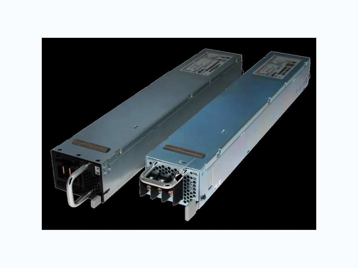
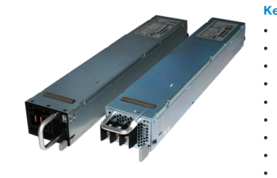
The PFE1100-12-054xD is a 1100 watt DC to DC power supply that converts DC input into a main output of 12 VDC for powering intermediate bus architectures (IBA) in high performance and reliability servers, routers, and network switches.
The PFE1100-12-054xD meets international safety standards and displays the CE-Mark for the European Low Voltage Directive (LVD).
Best-in-class, 80 PLUS certified “Platinum” efficiency
Best-in-class, “Platinum level” efficiency
Wide input voltage range: 40 – 72 VDC
Always-On 16.5 W programmable standby output (3.3 / 5 V)
Hot-plug capable
Parallel operation with active digital current sharing
High density design: 25.6 W/in3
Small form factor: 54.5 x 40 x 321.5 mm
I2C communication interface for control, programming and monitoring with PSMI and PMBus® protocol
- Overtemperature, output overvoltage and overcurrent protection
- 256 Bytes of EEPROM for user information
- 2 Status LEDs: IN OK and OUT OK with fault signaling
- High Performance Servers
- Routers
- Switches
Disclaimer: PMBus is a registered trademark of SMIF, Inc.

Page 2
2
Product Family
Power Level
Dash V1 Output Dash
Width
Input
N: Normal air flow R: Reverse air flow
PFE Front-Ends
1100 W
12 V
54 mm
D: DC
S: Screw type input connector / normal air flow T: Screw type input connector / reverse air flow

Vi nom Nominal input voltage
53
VDC
Vi Input voltage ranges
Normal operating (Vi min to Vi max)
40
72 VDC
Ii max Max input current
33 Arms
Ii p Inrush Current Limitation
Vi min to Vi max
60 Ap
Turn-on input voltage1 Vi on
Ramping up
42
45 VDC
Turn-off input voltage1 Vi off
Ramping down
37
40 VDC
Vi nom, 0.1∙Ix nom, Vx nom, TA = 25 °C
89.3
Vi nom, 0.2∙Ix nom, Vx nom, TA = 25 °C
93.5
η Efficiency without fan
%
Vi nom, 0.5∙Ix nom, Vx nom, TA = 25 °C
95
Vi nom, Ix nom, Vx nom, TA = 25 °C
92.9
Thold Hold-up Time
V1 > 10.8 V, VSB within regulation, Vi = 53 VDC, Px nom
5
ms
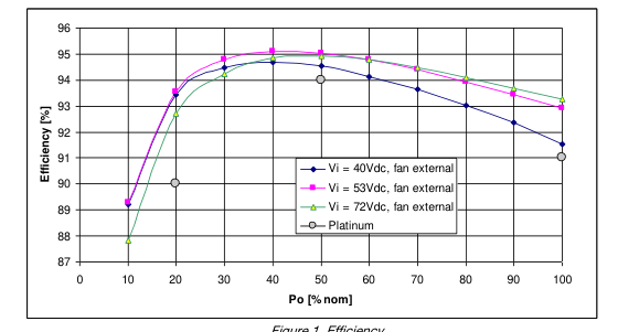
Figure 1. Efficiency
1 The Front-End is provided with a minimum hysteresis of 3 V during turn-on and turn-off within the ranges.

Page 3
3
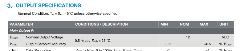
Vi min to Vi max,0 to 100% I1 nom,Ta min to Ta max
dV1 tot Total Regulation
-1
+1 % V1 nom
P1 nom Nominal Output Power
V1 = 12 VDC
1080
W
I1 nom Nominal Output Current
V1 = 12 VDC
90
ADC
V1 nom, I1 nom, 20 MHz BW,
v1 pp Output Ripple Voltage
150 mVpp
10nF/16V/X7R/1210 + 10uF/16V at V1
dV1 Load Load Regulation
Vi = Vi nom, 0 - 100 % I1 nom
80
mV
dV1 Line Line Regulation
Vi =Vi min…Vi max
10
mV
I1 max Current Limitation
95
105 ADC
dIshare Current Sharing
Deviation from I1 tot / N, I1 > 10%
-3
+3 A
dVdyn Dynamic Load Regulation
-0.6
0.6 V
ΔI1 = 50% I1 nom, I1 = 5 … 100% I1 nom, dI1/dt = 1 A/μs, recovery within 1% of V1 nom
Trec Recovery Time
1 ms
tAC V1 Start-Up Time From DC
V1 = 10.8 VDC
2 sec
tV1 rise Rise Time
V1 = 10…90% V1 nom
1
10 ms

Vi min to Vi max,0 to 100% ISB nom,Ta min to Ta max
dVSB tot Total Regulation
-2
+2 %VSBnom
PSB nom Nominal Output Power
VSB_SEL = 0 / 1
16.5
W
VSB = 3.3 VDC
5
ADC
ISB nom Nominal Output Current
VSB = 5.0 VDC
3.3
ADC
VSB nom, ISB nom, 20 MHz BW,
VSB pp Output Ripple Voltage
100 mVpp
10nF/16V/X7R/1210 + 10uF/16V at VSB
VSB_SEL = 1
67
mV
dVSB Droop
0 - 100 % ISB nom
VSB_SEL = 0
44
mV
VSB_SEL = 1
5.25
6 ADC
ISB max Current Limitation
VSB_SEL = 0
3.45
4.3 ADC
dVSBdyn Dynamic Load Regulation
-3
3 %VSBnom
ΔISB = 50% ISB nom, ISB = 5 … 100% ISB nom, dIo/dt = 0.5 A/μs, recovery within 1% of V1 nom
Trec Recovery Time
tAC VSB Start-Up Time From DC Input VSB = 90% VSB nom
tVSB rise Rise Time
VSB = 10…90% VSB nom
CLoad Capacitive Loading
Tamb = 25 °C

μs 250
2 sec
4
10 ms
μF 10000
North America
Asia-Pacific Europe, Middle East
+1 408 785 5200
+86 755 298 85888
+353 61 225 977
© 2018 Bel Power Solutions & Protection
BCD.00034_AI
Page 4
4
4.1 FRONT LEDS
IN LED (INPUT OK)
DC Line within range
DC Line UV condition
Redundant Operation - PSU1 operating and PSU2 has input power removed
OUT LED 2 (OUTPUT OK)
PSON High
Hot-Standby Mode
V1 or VSB out of regulation
Over temperature shutdown
Output over voltage shutdown (V1 or VSB)
Output over current shutdown (V1 or VSB)
Fan error (>15%)
Over temperature warning
Minor fan regulation error (>5%, <15%)
Redundant Operation - PSU1 operating and PSU2 has input power removed
1 The LEDs will be ON till input power from PSU1 is removed.
Solid Green
Off
Solid Yellow (PSU2) 1
Blinking Yellow (1:1)
Blinking Yellow/Green (1:2)
Solid Yellow
Blinking Yellow/Green (2:1)
Blinking Yellow/Green (1:1)
Off (PSU2)
2 The order of the criteria in the table corresponds to the testing precedence in the controller.
Table 1. LED Status
The front-end has 2 front LEDs showing the status of the supply. LED number one is green and indicates DC power is on or off, while LED number two is bi-colored: green and yellow, and indicates DC power presence or fault situations. For the position of the LEDs see Figure 5.

Page 5
5
4.2 GRAPHICAL USER INTERFACE
The Bel Power Solutions provides with its “I2C Utility” a Windows® XP/Vista/Win7 compatible graphical user interface allowing the programming and monitoring of the PFE1100-12-054xD Front-End.
The utility can be downloaded on www.belpowersolutions.com and supports both the PSMI and PMBus® protocols.
The GUI allows automatic discovery of the units connected to the communication bus and will show them in the navigation tree. In the monitoring view the power supply can be controlled and monitored.
If the GUI is used in conjunction with the PFE1100-12-054xD Evaluation Kit it is also possible to control the PSON pin(s) of the power supply.
Further there is a button to disable the internal fan for approximately 5 seconds (not implemented yet). This allows the user to take input power measurements without fan consumptions to check efficiency compliance to the Climate Saver Computing Platinum specification.
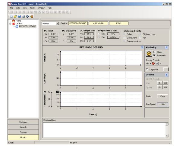
Figure 2. I2C Bus to uC (Graphical User Interface)
The monitoring screen also allows to enable the hot-standby mode on the power supply. The mode status is monitored and by changing the load current it can be monitored when the power supply is being disabled for further energy savings. This obviously requires 2 power supplies being operated as a redundant system (like the evaluation kit).
NOTE: The user of the GUI needs to ensure that only one of the power supplies have the hot-standby mode enabled.

North America
Asia-Pacific Europe, Middle East
+1 408 785 5200
+86 755 298 85888
+353 61 225 977
© 2018 Bel Power Solutions & Protection
BCD.00034_AI
Page 6
6
5.1 IMMUNITY
NOTE: Most of the immunity requirements are derived from EN 55024:1998/A2:2003.
IEC / EN 61000-4-2, ±8 kV, 25 + 25 discharges per test point
ESD Contact Discharge
B
(metallic case, LEDs, connector body) IEC / EN 61000-4-2, ±15 kV, 25 + 25 discharges per test point
ESD Air Discharge
B
(non-metallic user accessible surfaces) IEC / EN 61000-4-3, 10 V/m, 1 kHz / 80% Amplitude Modulation,
Radiated Electromagnetic Field
A
1 µs Pulse Modulation, 10 kHz…2 GHz IEC / EN 61000-4-4, Level 3
Burst
Input DC port ±1 kV, 1 minute
B
DC port ±0.5 kV, 1 minute IEC / EN 61000-4-5
Surge
Line to earth: ±1 kV
A
Line to line: ±0.5 kV
RF Conducted Immunity
IEC/EN 61000-4-6, Level 3, 10 Vrms, CW, 0.1 … 80 MHz
A
5.2 EMISSION

single unit, Vi = 53 VDC, Px nom
6 dB margin
Radiated Emission
Class A
EN55022 / CISPR 22: 30 MHz … 1 GHz, QP,
6 dB margin
2 units in rack system, Vi = 53 VDC, Px nom Sound power statistical declaration
Acoustical Noise
62 dBA
(ISO 9296, ISO 7779, IS9295) @ 50% load
TA Ambient Temperature
Vi min to Vi max, I1 nom, ISB nom
0
+45 °C
TAext Extended Temp. Range
Derated output
+45
+65 °C
Vi min to Vi max / I1 < 77 A, ISB nom
+55 °C
Vi min to Vi max / I1 < 35 A, ISB nom
+65 °C
TS Storage Temperature
Non-operational
-20
+70 °C
Na Audible Noise
Sound power @Vi nom, 50% Io nom, TA = 25°C
62
dBA
Width
54.5
Dimensions
Height
40
mm
Depth
321.5
M Weight
1.12
kg
NOTE: Tolerance (unless otherwise stated): 0 - 30 mm: +/- 0.2 mm; 30 - 120 mm: +/- 0.4 mm; 120 - 400 mm: +/-0.6 mm

Page 7
7
13.4
321.5 ±0.4
25
98
±0.4
9.5
80
Unlatching the supply is performed by pulling the green trigger in the handle.
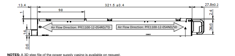
Figure 3. Side View 1
4.4
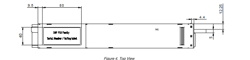
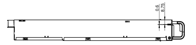
Figure 5. Side View 2
For additional information use other data files, or ask.
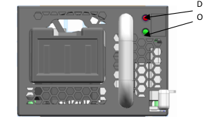
DC INPUT OK LED
All materials used, and finished product, must meet the requirements of the current RoHS directive 200
OUTPUT OK LED
Finish
Tolerances unles 0.5-30: ±0.1 Issued Modified
SNP Family Product GA
Mech. Eng. app Elec. Eng. appr Mfg. approved
Scale Dim. in mm
Size
Sheet Drawing No.
www.power-one.com
A3
3/4 SNP1100
Figure 6. Front View (PFE1100-12-054ND/RD)

North America
Asia-Pacific Europe, Middle East
+1 408 785 5200
+86 755 298 85888
+353 61 225 977
© 2018 Bel Power Solutions & Protection
BCD.00034_AI
Page 8
8
8.1 INPUT CONNECTOR
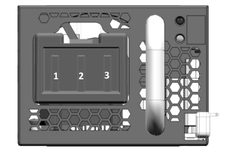
Unit: China Aviation (JOHNON OPTRONIC) P/N DP5ZJW0300-001 Counter part: China Aviation (JOHNON OPTRONIC) P/N DP5TJY0300-001(provided)
8.2 OUTPUT CONNECTOR
Input
1 Vin+ Input positive
2 Vin- Input negative
Ground 3 PE
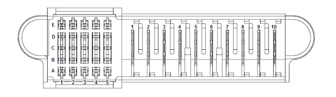
Unit: Tyco Electronics P/N 2-1926736-3 Counter part: Tyco Electronics P/N 2-1926733-5
NOTE: Column 5 is lagging (short pins)

Page 9
9
Output
+12 VDC main output
6, 7, 8, 9, 10 V1
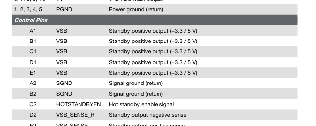
Standby output positive sense
E2 VSB_SENSE
I2C address and protocol selection (select by a pull down resistor)
A3 APS
B3 nc
Reserved
I2C data signal line
C3 SDA
Main output negative sense
D3 V1_SENSE_R
Main output positive sense
E3 V1_SENSE
I2C clock signal line
A4 SCL
Power supply on input (connect to A2/B2 to turn unit on)
B4 PSON
SMB Alert signal output
C4 SMB_ALERT
D4 nc
Reserved
E4 INOK
DC input OK signal
Power supply kill (lagging pin)
A5 PSKILL
Current share bus (lagging pin)
B5 ISHARE
Power OK signal output (lagging pin)
C5 PWOK
Standby voltage selection (lagging pin)
D5 VSB_SEL
Power supply present (lagging pin)
E5 PRESENT_L
Table 2. Pin Description

North America
Asia-Pacific Europe, Middle East
+1 408 785 5200
+86 755 298 85888
+353 61 225 977
© 2018 Bel Power Solutions & Protection
BCD.00034_AI
Page 10
10
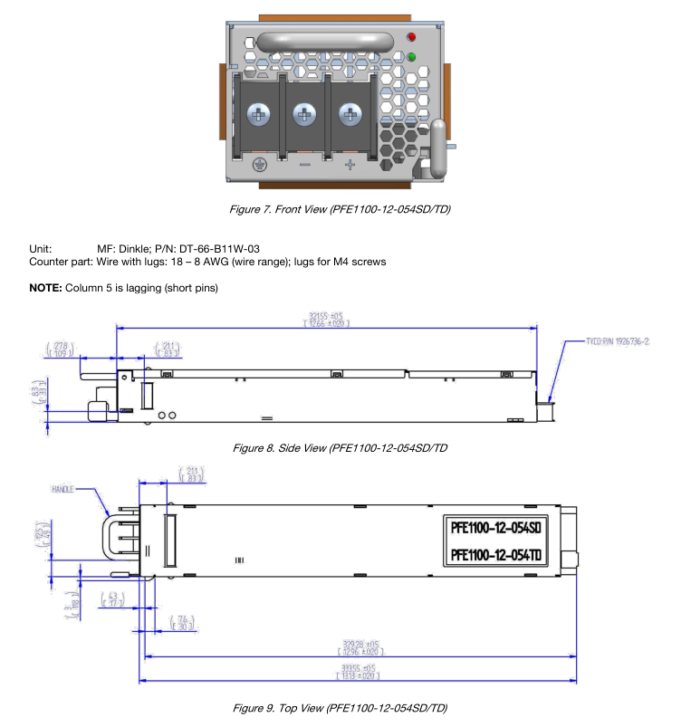
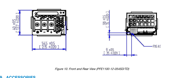
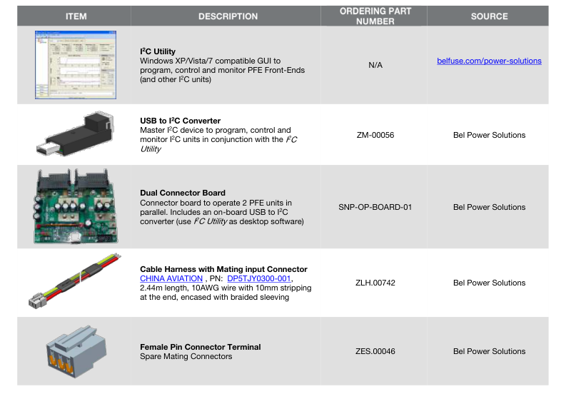
8.3 INPUT CONNECTOR MODIFICATION - MODELS PFE1100-12-054SD/TD

Page 11
11

North America
Asia-Pacific Europe, Middle East
+1 408 785 5200
+86 755 298 85888
+353 61 225 977
© 2018 Bel Power Solutions & Protection
BCD.00034_AI
Page 12
12
10.1
SOCKET CRIMPING OPERATION INSTRUCTION (DP5TJY0300-001)
I.
CRIMPING TOOLS AND MACHINE PREPARATION
Machine needed before crimping: Terminal Crimping Machine, Crimping Mould, Crimping Tools, Wire Strippers, Utility Knife and Wrench.
NOTES: 1.Crimping tool need to install onto crimping mould, and crimping mould need to fix onto crimping machine. 2. Two factors must be considered during the design of crimping mould: A: must meet dimensions of tools installation. B: Easy to install in machine and be in machine effective itinerary
NAME
SUPPLIER
PART NUMBER
Terminal Crimping Machine
JonHon Optronic
THB Terminal Crimping Machine
Crimping Mould
JonHon Optronic
12A-01
Crimping tools
JonHon Optronic
YJD-DP5
Crimping tools YJD-DP5 including 4 parts: 4U-A5881-1, 4U-A5881-2, 4D-A5881-1, 4D-A5881-2. (See picture 1)
Table 1. A Set of Machine Recommended
II.
CRIMPING MACHINE AND TOOLS INSTALLATION
Crimping mould and crimping tools must be installed well before crimping.
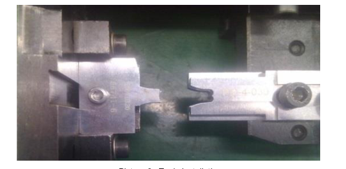
Install Requirements: 1. Up tools 4U-A5881-1 and 4U-A5881-2 need install in dynamic mould. Down Tools 4D-A5881-1 and 4D-A5881-2 need install in static mould. (See picture 2) 2. 4 pieces crimping tools can divieded into 2 pairs: 4U-A5881-1 mated with 4D-A5881-1, which is crimping cable jacket. 4U-A5881-2 match 4D-A5881-2, which is crimping cable core. 3. Up tool 4U-A5881-1 has U-shaped hole. Customer can adjust the install position according to wire thickness, which to make sure the wire jacket and core will be crimping tightly. Tool 4D-A5881-1 need to install outside of crimping mould, in order to adjust tool 4U-A5881-1. (Reference at Picture 2)
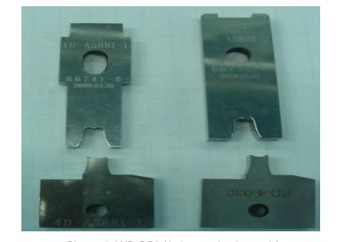
Picture 1. YJD-DP5 (4 pieces crimping tools)

Page 13
13
Picture 2. Tools Installation
III.
CRIMPING
- Wire Cutting: Cutting wire with required length, and the wire can be used 8AWG American standard wire or other 8mm2 wire. 2. Wire Stripping: Stripping the wire jacket 8±1mm with Wire Strippers, and cutting the jacket straight with Utility Knife. The wire should be at the set of bundles after stripping, shown as Picture 3.


Picture 4. Wire and Terminal before Crimping
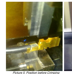
- Crimping: Placing the wire and the terminal shown as picture 4, and placing them into the gap between up tool and down tool shown as picture 5.

North America
Asia-Pacific Europe, Middle East
+1 408 785 5200
+86 755 298 85888
+353 61 225 977
© 2018 Bel Power Solutions & Protection
BCD.00034_AI
Page 14
14
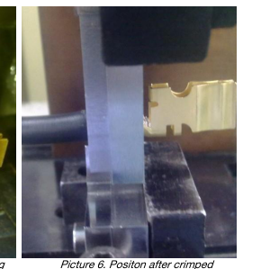
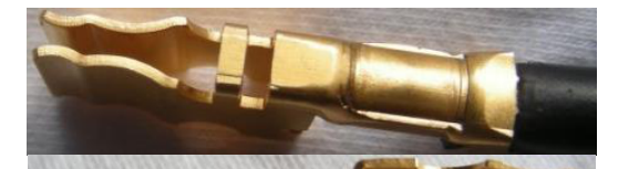
- Start the terminal crimping machine, and crimping closed shown as picture 6. 5. Test after Crimping Appearance Inspection: The crimped position should be smooth and firm. (reference see picture 7) a)
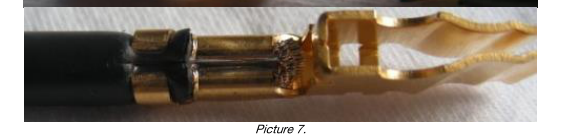
If the severe deformation after crimping, we need to adjust the machine knob to adjust the crimping mould and distance between up tool and down tool, which to ensure the crimp the wire correctly and beautifully. Meanwhile, we need to avoid too much crimping strength so as to short the tools life, or even to damage the tools.
b) Pulling-Out Force Test: When the first batch after a terminal crimping, crimp pull out force should be inspected Test Method: Fixed the terminal and Non-crimped wire onto ends of tension meter, and then gradually increase the tension until the wire is pulled and separated from the terminal, and read the tension meter reading is to pull off the greatest force. Qualification Criterion: When the pull-out force meets the requirements of Table 2, and then can show pull-out force is qualified. Failure Treatment: When the pull-out force failed, we need to adjust the machine knob to adjust the crimping mould and distance between up tool and down tool, and then re-crimp until the test qualified. After that, we can
make mass production.

Page 15
15
CABLE SIZE
CORE CROSS-SECTIONAL AREA
PULL-OUT FORCE
8.5 mm2
8 AWG
950 N
5.5 mm2
10 AWG
650 N
Table 2. Pull-Out Force Table
NOTE: Mid-value clustering Method will be used if core cross-sectional area is not in the range of Table 2
IV.
TREATMENT AFTER CRIMPING
Crimping tools, crimping mould should be removed from crimping machine and properly kept after crimping work.
10.2
INPUT CONNECTOR DATASHEET (DP5ZJW0300-001/DP5TJY0300-001)
▪ Material Code: ▪ Part Name: DP5ZJW0300-001 3pin PCB receptacle, DP5TJY0300-001 3 pin crimp plug ▪ Part Number: Receptacle (fix connector) DP5ZJW0300-001
Plug (moving connector) DP5TJY0300-001 ▪ Information of environment protection: compliant with ROHS
▪ Technical Parameter Mated:
- Electrical
o Current rating: 40 A at 55℃ (accord with UL1977) o Withstanding voltage: 1500 V o Insulation Resistance ≥ 500 MΩ (Normal temperature); ≥ 100 MΩ (Damp Heat) o Hot plug function: Can meet the over load requirement of UL1977
- Mechanical Characteristics
o Terminal type: receptacle PCB, plug crimp o Service life: 250 cycles
- Material and Surface Treatment
o Contact material sockets: Copper alloy; pins: Copper Surface Treatment:0.2~0.6 μm gold plated over 1.27 μm nickel (or 5 um silver, up to customer requirement) o Housing material & processing Material: glass fiber strengthened flameless PET UL94V-0 Color: black Processing method: plastic injection
- Operating Environment
o Range of temperature: -55℃~125℃ o Humidity: 93% at 40℃ o Shock acceleration 490 m/s2 o Vibration: 10Hz~2000 Hz, acceleration: 98 m/s2
- Dimensions of Product
o Dimension

North America
Asia-Pacific Europe, Middle East
+1 408 785 5200
+86 755 298 85888
+353 61 225 977
© 2018 Bel Power Solutions & Protection
BCD.00034_AI
Page 16
16
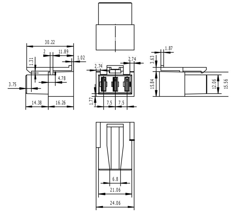
Picture 8. Receptacle: DP5ZJW0300-001
NUCLEAR AND MEDICAL APPLICATIONS - Products are not designed or intended for use as critical components in life support systems, equipment used in hazardous environments, or nuclear control systems. TECHNICAL REVISIONS - The appearance of products, including safety agency certifications pictured on labels, may change depending on the date manufactured. Specifications are subject to change without notice.