
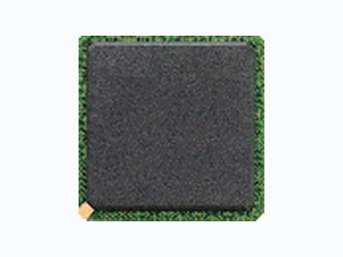
PEX8111 ETC1
Document overview
- Manufacturer or author: Provided By www.digicamel.com(FREE DATASHEET DOWNLOAD SITE)
- PDF pages: 2
Technical content
Features
General Features o Forward and Reverse bridging o Tiny 161 ball BGA package (10mm x 10mm) o Low power – 0.3 Watts maximum o EEPROM configuration option with SPI o Internal 8Kbyte shared RAM o 1.5 V core supply voltage o JTAG o Four (4) GPIO pins for maximum design and application flexibility o Extensive PME support including D0 and D0 Active, D1, D2 and D3Hot and D3Cold Integrated PCI Express Interface o PCI Express Base specification 1.0a compliant o x1 Link, full-duplex, 2.5 Gbps o One virtual channel o Automatic LVDS polarity reversal o 128 byte maximum payload size o Link CRC o Link power management o Flow control buffering o PCI Express transaction queues for eight (8) outstanding TLPs PCI Interface o PCI 3.0: 32 bits at 33 MHz o PCI Power Management 1.1 o Internal arbiter supports up to 4 external masters; provides REQ#/GNT# signals o 3.3V I/O and 5V tolerant PCI o Message Signal Interrupt (MSI) support o Provides PCI clock output o Four mailbox registers for messaging o ISA Enable and VGA Enable registers for legacy operation Reversible Bridge in a Tiny Package The PLX Technology PEX 8111 bridge enables designers to migrate legacy PCI bus interfaces to the new advanced serial PCI Express. This is ideal when including existing PCI ICs on a PCI Express™ Adapte r Board, such as the new ExpressCard™ standard. This simple bridge can also reside on either end of a PCI Express cable to connect remote functions running the PCI protocol. The PEX 8111 supports forward and reverse bridging. The tiny 10 mm x 10mm Plastic BGA package makes the PEX 8111 bridge ideal for use in applications where board real estate is at a premium. With its low power 0.15 micron CMOS design, the PEX 8111 consumes a maximum power of only 300 mW. Forward and Reverse Bridging Compliant to the PCI Express-to-PCI/PCI-X Bridge Specification 1.0, the PEX 8111 is capable of operating in either forward or reverse bridging modes. In forward mode, the bridge allows legacy PCI chips and adapters to be used with new PCI Express processor systems. Reverse bridge operation allows conventional PCI processors and chipsets to configure and control advanced PCI Express switches and endpoints. The reverse PEX 8111 not only allows complete configuration of a downstream PCI Express system from the PCI bus, but it also handles limited PCI Express root functions for reverse interrupt and Power Management Events. Block Diagram The PEX 8111 is equipped with a standard PCI Express port that operates as a single, x1 link with a maximum of
250 Megabytes per second of throughput
per transmit and receive direction. With a single 2.5 Gbps integrated SerDes, the standard PCI Express signaling delivers the highest bandwidth with the lowest possible pin count using LVDS technology. The PEX 8111 has a single parallel bus segment supporting the PCI v 3.0 protocol. With a 32-bit wide parallel data path running at 33MHz, the PCI bandwidth is 132 Megabytes per second. While the PCI Express link accommodates the full PCI bus bandwidth, the device also supports internal queues with flow control features to optimize throughput and traffic flow. Figure 1. PEX 8111 Block Diagram