Download PDF
PET1300-12-054XA BEL
Document overview
- PDF pages: 23
Technical content
Page 1

PET1300-12-054xA is a 1300 Watt AC to DC power-factor-corrected (PFC) power supply that converts standard AC mains power into a main output of 12 VDC for powering intermediate bus architectures (IBA) in high performance and reliability servers, routers, and network switches.
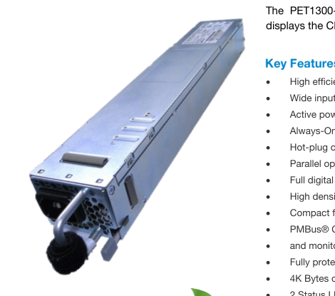
The PET1300-12-054xA meets international safety standards and displays the CE-Mark for the European Low Voltage Directive (LVD).
High efficiency up to 94.0%
Wide input voltage range: 90 – 264 VAC
Active power factor correction
Always-On 10 W standby output (3.3 V)
Hot-plug capability
Parallel operation with active current sharing
Full digital control for circuit loop and power management
High density design: 30.25 W/in3
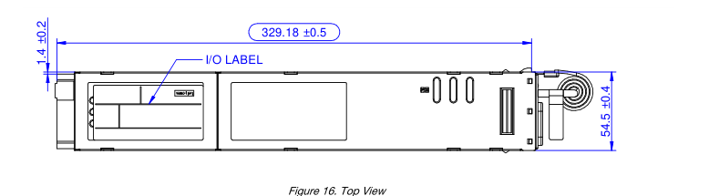
Compact form factor: 54.5 x 40.0 x 321.5 mm
PMBus® Communication Interface for control, programming
Fully protected (OTP, OCP, OVP, SCP)
4K Bytes of EEPROM for user information
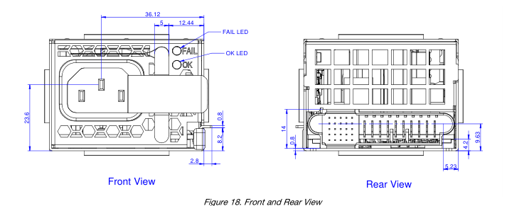
- 2 Status LEDs: FAIL and OK with fault signaling
- Approved to the latest edition of following Safety Standards: UL/CSA60950-1, IEC / EN 60950-1
- High Performance Servers
- Networking Switches
- Routers
Disclaimer: PMBus is a registered trademark of SMIF, Inc.

Page 2
2
PET
1300
-
12
-
054
x
A
Product Family
Power Level Dash
V1 Output
Dash
Width
Airflow
Input
N: Normal
PET Front-Ends
1300 W
12 V
54 mm
A: AC
R: Reverse
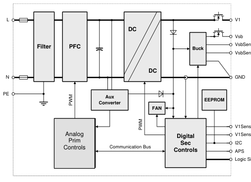
The PET1300-12-054xA AC/DC power supply is a fully DSP controlled, highly efficient front-end power supply. It incorporates resonance-soft-switching technology and interleaved power trains to reduce component stresses, providing increased system reliability and very high efficiency. With a wide input operational voltage range and minimal linear derating of output power with input voltage and temperature, the PET1300-12-054xA maximizes power availability in demanding server, network, and other high availability applications. The supply is fan cooled and ideally suited for integration with a matching airflow paths.
The PFC stage is an analogue solution; MCU is used to communicate with DSP chip on secondary side.
The DC/DC stage uses soft switching resonant techniques in conjunction with synchronous rectification. An active OR-ing device on the output ensures no reverse load current and hence it is ideally suited for operation in redundant power systems.
The always-on standby output with voltage level (3.3 Volts), provides power to external power distribution and management controllers. It is protected with an active OR-ing device for maximum reliability.
Status information is provided with front-panel LEDs. In addition, the power supply can be controlled and the fan speed set via the I2C bus. The I2C bus allows full monitoring of the supply, including input and output voltage, current, power, and inside temperatures.
Cooling is managed by a fan controlled by the DSP controller. The fan speed is adjusted automatically depending on the actual power demand and supply temperature and can be overridden through the I2C bus.
Logic Signals
Figure 1. PET1300-12-054xA Block Diagram

Page 3
3

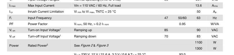
Vi Input Voltage Ranges
Normal operating (Vi min to Vi max)
90
264 VAC
Vin = 230 V, 12 V / 21.6 A, 3.3 V / 0.6 A TA = 25 °C
93.0
η Efficiency without Fan
Vin = 230 V, 12 V / 54 A, 3.3 V / 1.5 A TA = 25 °C
94.0
%
Vin = 230 V, 12 V / 108 A, 3.3 V / 3 A TA = 25 °C
92.0
After last AC zero point, V1 > 11.6 V, VSB within
Thold Hold-up Time
10
ms
regulation, Vi = 230 VAC, 12 V / 108 A, 3.3 V / 3 A
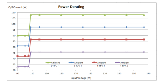
Figure 2. Derating on Iout vs Vin and Ta for PET1300-12-054NA
1 The Front-End is provided with a minimum hysteresis of 3 V during turn-on and turn-off within the ranges. 2 The output power is should be derating as below curve if operation temperature increases from 45°C to 60°C.

Page 4
4
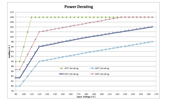
Figure 3. Derating on Iout vs Vin and Ta for PET1300-12-054RA
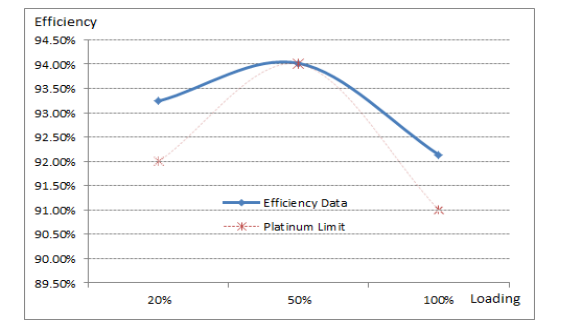
Figure 4. Efficiency Measurement Curve

Page 5
5
General Condition: TA = 0… 60 °C, unless otherwise noted.
PARAMETER
DESCRIPTION / CONDITION
MIN NOM MAX
UNIT
Main Output V1
V1 nom Nominal Output Voltage
12.0
VDC
0.5 ∙I1 nom, Tamb = 25 °C
V1 set Output Setpoint Accuracy
-0.5
+0.5 % V1 nom
dV1 tot Total Regulation
Vi min to Vi max, 0 to 100% I1 nom, Ta min to Ta max
-3
+3 % V1 nom
P1 nom Nominal Output Power
V1 = 12 VDC
1296
W
V1 = 12 VDC, Vin ≥ 108 VAC
I1 nom Nominal Output Current
108
ADC
v1 pp Output Ripple Voltage
V1 nom, I1 nom, 20 MHz BW
180 mVpp
dV1 Load Load Regulation
Vi = Vi nom, 0 - 100% I1 nom
60
mV
dV1 Line Line Regulation
Vi =Vi min…Vi max
20
mV
Current Sharing
when Bus load ≥ 27 A
4.5 A
dIshare (abs (I1-I2), between any two
when Bus load < 27 A
5.6 A
units in parallel)
dVdyn Dynamic Load Regulation
-0.6
0.6 V
Iout:10%--60% of full load; 50%--100% of full load dI1/dt = 1A/μs, recovery within 1% of V1 nom
Trec Recovery Time
0.5 1 ms
tAC V1 Start-up Time from AC
2 s
tV1 rise Rise Time
V1 = 10…90% V1 nom
3
ms
µF
CLoad Capacitive Loading
Ta = 25 °C
11000
Standby Output VSB
VSB nom Nominal Output Voltage
3.3
VDC
0.5 ∙ISB nom, Tamb = 25 °C
VSB set Output Setpoint Accuracy
-1
+1 %V1nom
dVSB tot Total Regulation
Vi min to Vi max, 0 to 100% ISB nom, Ta min to Ta max
-1.5
+1.5 %VSBnom
PSB nom Nominal Output Power
VSB = 3.3 VDC, normal airflow
10
W
ISB nom Nominal Output Current
VSB = 3.3 VDC, normal airflow
3
ADC
VSB pp Output Ripple Voltage
VSB nom, ISB nom, 20 MHz BW (See Section 5.1)
45 mVpp
dVSB Droop
0 - 100% ISB nom
67
mV
dVSBdyn Dynamic Load Regulation
-3
3 %VSBnom
ΔISB = 50% ISB nom, ISB = 5 … 100% ISB nom, dIo/dt = 0.5 A/μs, recovery within 1% of V1 nom
µs
Trec Recovery Time
250
tAC VSB Start-up Time from AC
3 s
tVSB rise Rise Time
VSB = 10…90% VSB nom
4 20 ms
µF
CLoad Capacitive Loading
Tamb = 25 °C
1000

Page 6
6
General Condition: TA = 0… 60 °C, unless otherwise noted.
PARAMETER
DESCRIPTION / CONDITION
MIN
NOM MAX
UNIT
F Input Fuses (L+N)
Not user accessible, quick-acting (F)
16
A
V1 OV OV Threshold V1
13.5
14.5 VDC
tOV V1 OV Latch Off Time V1
1 ms
VSB OV OV Threshold VSB
3.6
4.3 VDC
tOV VSB OV Latch Off Time VSB
1 ms
IV1 lim Current Limit V1
See Figure 5 & Figure 6
112 115 117 ADC
Isb lim Current Limit V1 Tamb = 25 °C
Standby output can recover.
4.5 A
IV1 SC Max Short Circuit Current V1
150
A
tV1 SC Short Circuit Regulation Time
V1 < 3 V, time until IV1 is limited to < IV1 sc
2
ms
tV1 SC off Short Circuit Latch Off Time
Time to latch off when in short circuit
500
ms
TSD Over Temperature on Heat Sinks Automatic shut-down
115
°C
NOTE: The OCP should be derating as below curve if operation temperature increases from 45°C to 60°C, And OCP warning is before 2 A than OCP set point.
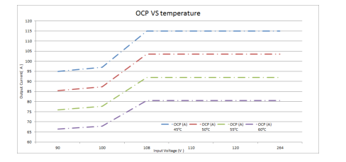
Figure 5. Vin vs Output Current for PET1300-12-054NA
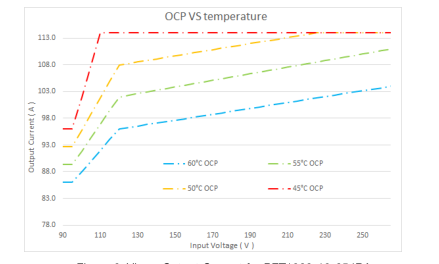
Figure 6. Vin vs Output Current for PET1300-12-054RA

Page 7
7
6.1 FRONT LEDs
The front-end has 2 front LEDs showing the status of the supply. LED number one is green which indicates presence of AC power, LED number two is bi-colored: green and yellow, which indicates DC power presence or fault. For the position and states of the LEDs see Table 2.
POWER SUPPLY CONDITION
No AC power to all power supplies Power Supply Failure (includes over voltage, over current, over temperature and fan failure) Power Supply Warning events where the power supply continues to operate (high temperature, high power and slow fan) AC Present / 3.3 VSB on (PSU OFF)
Power Supply ON and OK
Table 1. LED Status
GREEN (OK)
AMBER (FAIL)
LED STATUS
LED STATUS
OFF
OFF
OFF
ON
OFF
1 Hz Blinking
1 Hz Blinking
OFF
ON
OFF
NOTE: When unit see fan failure, unit will shut down and can only be restarted by using PSON_L signal or AC input power recycling or PMBus® commands. Refer to software specification for detail.
6.2 ELECTRICAL CHARACTERISTICS
General Condition: TA = 0… 60 °C, unless otherwise noted.
PARAMETER DESCRIPTION / CONDITION
MIN NOM MAX
UNIT
PSKILL_H/PSON_L/PRESENT_L
VIL
Input Low Level Voltage
0
0.8 V
VIH
Input High Level Voltage
2.0
3.6 V
IIL, H
Maximum Input Sink or Source Current
0
1 mA
kΩ
RpuSKILL_H
Internal Pull Up Resistor on PSKILL_H
10
kΩ
RpuPSON_L
Internal Pull Up Resistor on PSON_L
10
kΩ
RpuPRESENT_L
Internal Pull Up Resistor on PRESENT_L
None
kΩ
RLOW
Resistance Pin to SGND for Low Level
0
1
kΩ
RHIGH
Resistance Pin to SGND for High Level
50
PWOK_H Output
Vext
Maximum External Pull Up Voltage
3.6 V
VOL
Output Low Level Voltage
Isink < 2 mA
0
0.4 V
VOH
Output High Level Voltage
Isource < 0.5 mA
2.4
3.6 V
kΩ
RpuPWOK_H
Internal Pull Up Resistor on PWOK_H
None
ACOK_H Output
Vext
Maximum External Pull Up Voltage
3.6 V
VOL
Output Low Level Voltage
Isink < 2 mA
0
0.4 V
VOH
Output High Level Voltage
Isource < 0.5 mA
2.4
3.6 V
kΩ
RpuACOK_H
Internal Pull Up Resistor on ACOK_H
None
SMB_ALERT_L Output
Vext
Maximum External Pull Up Voltage
12 V
VOL
Output Low Level Voltage
Isink < 2 mA
0
0.4 V
IOH
Maximum High Level Leakage Current
10 µA
kΩ
RpuSMB_ALERT_L Internal Pull Up Resistor on SMB_ALERT_L
None

Page 8
8
6.3 GRAPHICAL USER INTERFACE
Bel Power Solutions provide with its “Bel Power Solutions I2C Utility” a Windows® XP/Vista/Win7 compatible graphical user interface allowing the programming and monitoring of the PET1300-12-054xA Front-End. The utility can be downloaded on belfuse.com/power-solutions and supports both the PSMI and PMBus® protocols. The GUI allows automatic discovery of the units connected to the communication bus and will show them in the navigation tree. In the monitoring view the power supply can be controlled and monitored.
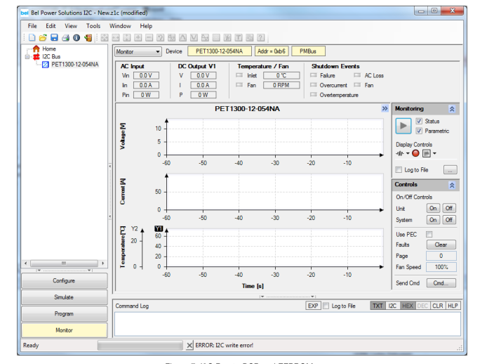
Figure 7. I2C Bus to DSP and EEPROM
20% ~ 100% FULL LOAD
COMMAND
10% ~ 20% FULL LOAD
REMARK
Read_Iin
< 0.5 A
+/- 3%
It is for corresponding to max input current
Read_Iout
+/- 2%
+/- 2%
It is for corresponding to max output current
Read_Vin
+/- 3%
+/- 2.5 V
Read_Vout
+/- 2%
+/- 2%
Read_Pin
---
+/- 15%
It is for corresponding to max input power
Read_Pout
+/- 3%
+/- 3%
It is for corresponding to max output power
Table 2. Accuracy for PMBus®

Page 9
9
6.4 PRESENT_L
The PRESENT_L is an output signal and it is used to sense the number of power supplies in the system (operational or not). This signal is connected to the power supply’s output ground. Electrical characteristics see 6.2.
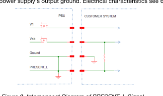
Figure 8. Interconnect Diagram of PRESENT_L Signal
6.5 SMB_ALERT_L
The SMB_ALERT_L is an output signal and shall be an open collector with the pull-up resistor located at the receiving end and shall capable of sinking up to 4 mA. This signal indicates that the power supply is experiencing a problem that the user should investigate. This may be asserted due to Critical events or Warning events. See PMBus® specification for further details.
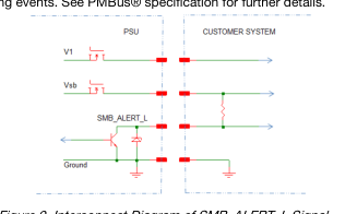
Figure 9. Interconnect Diagram of SMB_ALERT_L Signal
6.6 PSKILL_H
This is an input signal and is used to force the 12 V main output off if the supply is removed from the system. At the system level this pin will be connected to the output return directly. When this input is low the power supply will operate. If the input is floating the 12 V main output will turn off while the 3.3 VSB will remain on. This signal overrides all other on-and-off signals. On the power supply connector, this pin is shorter than the others so it is a last-make and first-break contact. See below Table 3 for Logic Table.
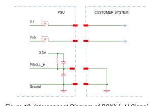
Figure 10. Interconnect Diagram of PSKILL_H Signal

Page 10
10
SIGNAL CHARACTERISTICS
Accepts a ground input from the system.
Signal Type:
Pull-up to 3.3 VSB located in the power supply.
Input Signal to the power supply PS_KILL = Low, PS_ON = Low
ON
PS_KILL = Open, PS_ON = Low or Open
OFF
PS_KILL = Low, PS_ON = Open
OFF
MIN
MAX
Source current, Vps_kill =Low
4 mA
Table 3. PS_ON_L Signal Characteristics
6.7 PSON_L
The PS_ON_L signal is an input signal used to remotely turn on/off the power supply. PS_ON_L is an active LOW signal that turns on the 12 V main output. In the low state this input will not source more than 4 mA of current. The 12 V output will be disabled when this input is driven HIGH, or open circuited. See Table 4 for Logic Table.
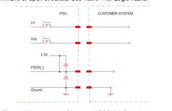
Figure 11. Interconnect Diagram of PSON_L Signal
SIGNAL CHARACTERISTICS
Accepts an open collector/drain input from the system. Pull-up to 3.3 VSB
Signal Type: Input signal to the power supply
located in power supply.
PS_ON_L = Low, PS_KILL = Low
ON
PS_ON_L = Open, PS_KILL = Low or Open
OFF
PS_ON_L = Low, PS_KILL = Open
OFF
MIN
MAX
Output Source Current, VPS_ON_L= Low
4 mA
Table 4. PS_ON_L Signal Characteristics
6.8 PW_OK
PW_OK is an output signal and will be pulled HIGH by the power supply to indicate that all the outputs are within the regulation limits of the power supply. When 12 V main output is < 10.9 V or > 13.2 V, or if any of the outputs fail due to over current protection, over voltage protection, over temperature, or fan failure then this output will be driven LOW. In the event when AC mains power is lost, this signal will be driven LOW at least 20 ms before the +3.3 VSB output is lost. The output will be an open collector/drain. The start of the PW_OK delay time shall be inhibited as long as any power supply’s 12 V output is in current limit. See Table 5.

Page 11
11
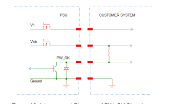
Figure 12. Interconnect Diagram of PW_OK Signal
SIGNAL CHARACTERISTICS
Open collector/drain (system side to provide pull-up, another pull-up to
Signal Type:
3.3 VSB could also be located in the power supply)
Output signal from the power supply PW_OK = High
Power OK
PW_OK = Low
Power Not OK
MIN
MAX
Input Sink current, PW_OK = Low
4 mA
Output Source current, PW_OK = High
2 mA
Table 5. PW_OK Signal Characteristics
6.9 AC_OK
This signal is an output signal and will be asserted, driven HIGH, by the power supply to indicate that the input voltage meets the minimum requirements of Section 3.1.3. After falling outside the input voltage requirements for more than 20 ms, the signal must be driven LOW. The output will be an open collector/drain. See below Table 6.
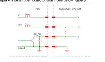
Figure 13. Interconnect Diagram of AC_OK Signal
SIGNAL CHARACTERISTICS
Open collector/drain (system side to provide pull-up, another pull-up to
Signal Type:
3.3 VSB could also be located in the power supply)
Output signal from the power supply AC_OK = High
AC OK
AC_OK = Low
AC Low (Not OK)
MIN
MAX
Input Sink current, AC_OK = Low
4 mA
Output Source current, AC_OK = High
2 mA
Table 6. AC_OK Signal Characteristics

Page 12
12
6.10
CURRENT SHARING
All outputs shall be capable of operating in a redundant current share mode. A maximum of 6 power supplies may be operated in parallel. All outputs shall incorporate an isolation device (Or-ing MOSFET or diode) for fault isolation. Filter capacitors that are located after the isolation device shall be of high reliability and shall be de-rated sufficiently to minimize failures. The 3.3 V output current sharing shall be of a droop type. The +12 V current sharing shall be a single wire type, active current sharing. Connecting the Ishare (current share) pins of each power supply together shall enable the current share feature. Shorting or opening of a current share pin shall not cause the output voltage to go out of steady state regulation.
For 12 V output the Ishare (load sharing) voltage shall be a linear function Ishare [V] = 8 x Iout/108 (with 8 V at 108 A) for a single power supply (~74 mV/A). At light load, the load share becomes difficult because of low feedback signal. Refer to Table 2 for current sharing accuracy. The current balance accuracy is calculated as: 2\*|I1-I2|/ (I1+I2), where the I1 is the PSU1 load current and I2 is the PSU2 load current.
6.11
REMOTE SENSE
The outputs specified shall incorporate remote sense and will compensate for specified load cable drop. In the event of loss of remote sense, all outputs shall revert to internal sense so as to limit the outputs to less than 105% of nominal.

Page 13
13
Unless defined otherwise, all control signals shall be TTL compatible with respect to the output return and shall be isolated from the primary circuit and be SELV rated. All input signals shall be driven from an open collector with the pull-up resistor located in the power supply and shall be capable of sourcing up to 4 mA. General LVTTL signal levels are specified in below table except where explicitly specified otherwise.
PARAMETER
SYMBOL
MIN MAX
UNITS
Output High Voltage
Voh
2.4 3.6
V
Output Low Voltage
Vol
0 0.4
V
Input High Voltage
Vih
2.0 3.6
V
Input Low Voltage
Vil
0 0.8
V
Table 7. Low-Voltage TTL (LVTTL) Voltage Levels
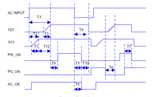
Figure 14. Timing Diagram
PARAMETER
CONDITION / COMMENTS
MIN TYP MAX UNITS
T1 (Tout_rise)
Output voltage rise time from each main output
0.5
100 ms
T2 (Tsb_on_delay)
Delay from AC being applied to 3V3 being within regulation
2500 Ms
T3 (Tac_on_delay)
Delay from AC being applied to all output voltages being within regulation
3000 ms
T4 (Tvout_holdup)
Time all output voltages, including 3V3, stay within regulation after loss of AC
10
ms
T5 (Tpw_ok_holdup)
Delay from loss of AC to de-assertion of PW_OK
5
ms
T6 (Tps_on_delay)
Delay from PS_ON_L active to output voltages within regulation limits
5
400 ms
T7 (Tps_on_pw_ok)
Delay from PS_ON_L de-active to PW_OK being de-asserted
50 ms
T8 (Tac_ok_off)
Delay from loss of AC input to de-assertion of AC_OK
20 ms
T9 (Tpw_ok_on)
Delay from output voltages within regulation limits to PW_OK asserted at turn on
100
1000 ms
T10 (Tpw_ok_off_12V) Delay from PW_OK de-asserted to 12 VDC dropping out of regulation limits
1
700 ms
T11 (Tpw_ok_off_3V3) Delay from PW_OK de-asserted to 3V3 dropping out of regulation limits
20
ms
T12 (Tsb_vout)
Delay from 3V3 being in regulation to 12 VDC being in regulation at AC turn on.
50
1000 ms
T13 (Tac_ok_on)
Delay from AC being applied to assertion of AC_OK
1500 ms

Page 14
14
8.1 IMMUNITY
PARAMETER
DESCRIPTION / CONDITION
CRITERION
IEC / EN 61000-4-2, ±8 kV, 25+25 discharges per test point
ESD Contact Discharge
A
(metallic case, LEDs, connector body) IEC / EN 61000-4-2, ±15 kV, 25+25 discharges per test point
ESD Air Discharge
A
(non-metallic user accessible surfaces) IEC / EN 61000-4-3, 10 V/m, 1 kHz/80% Amplitude Modulation,
Radiated Electromagnetic Field
A
1 µs Pulse Modulation, 10 kHz…2 GHz IEC / EN 61000-4-4, level 3
Burst
AC port ±2 kV, 1 minute
A
DC port ±1 kV, 1 minute IEC / EN 61000-4-5
Surge
4 kV CM
A
2 kV DM
RF Conducted Immunity
IEC/EN 61000-4-6, Level 3, 10 Vrms, CW, 0.1 … 80 MHz
A
IEC/EN 61000-4-11 1: Vi 230 V, 100% Load, Phase 0 °, Dip 100%, Duration 10 mS
A
Voltage Dips and Interruptions
2: Vi 230 V, 100% Load, Phase 0 °, Dip 100%, Duration 20 mS
VSB: A, V1: B
3: Vi 230 V, 100% Load, Phase 0 °, Dip 100%, Duration > 20 mS
VSB, V1: B
NOTE: Most of the immunity requirements are derived from EN 55024: 1998/A2:2003.
8.2 EMISSION
PARAMETER
DESCRIPTION / CONDITION
CRITERION
EN55022 / CISPR 22: 0.15 … 30 MHz, QP and AVG, single unit
Class A
Conducted Emission
EN55022 / CISPR 22: 0.15 … 30 MHz, QP and AVG, 2 units in rack system
Class A
EN55022 / CISPR 22: 30 MHz … 1 GHz, QP, single unit
Class A
Radiated Emission
EN55022 / CISPR 22: 30 MHz … 1 GHz, QP, 2 units in rack system
Class A
IEC61000-3-2, Vin = 115 VAC / 60 Hz, & Vin = 230 VAC/ 50 Hz, 100% Load
Harmonic Emissions
Class A
Acoustical Noise
46 dBA at 1 meter, 25 °C, 50% Load
-
AC Flicker
IEC61000-3-3, Vin = 230 VAC / 60 Hz, 100% Load
Pass
Maximum electric strength testing is performed according to UL / CSA 60950-1, IEC/EN 60950-1. Input-to-output electric strength tests should not be repeated in the field. Bel Power Solutions will not honor any warranty claims resulting from electric strength field tests.
PARAMETER
DESCRIPTION / CONDITION
Approved to the latest edition of the following standards:
Agency Approvals
UL / CSA 60950-1 IEC / EN 60950-1 Input (L/N) to case (PE)
Isolation Strength
Input (L/N) to output
Output to case (PE)
Input to case
Electrical Strength Test
Input to output

MIN NOM
MAX UNIT
Approved by independent body (see CE Declaration) Basic
Reinforced
Functional
2121
VDC
4242
Page 15
15
PARAMETER
DESCRIPTION / CONDITION
MIN NOM MAX
UNIT
TA Ambient Temperature
Vi min to Vi max, I1 norm, ISB nom
0
+60 °C
TS Storage Temperature
Non-operational
-40
+85 °C
Altitude
Operational, above Sea Level
-
10,000 Feet
Na Audible Noise
Vi = 230 VAC, 50% Io nom, TA = 25°C
46
dBA
NOTE: Refer to Figure 2 & 3 for Derating.
PARAMETER
DESCRIPTION / CONDITION
MIN NOM MAX
UNIT
Width
54.1 54.5 54.9
Dimensions
Height
39.6 40.0 40.4 mm
Depth
321.1 321.6 322.1
M Weight
1.09
kg
NOTES: Tolerance: 0.5 mm – 120 mm: ±0.3 mm; 120 mm – 400 mm: ±0.5 mm. A 3D step file of the power supply casing is available on request.

Figure 15. Side View 1

Page 16
16

Figure 17. Side View 2

Page 17
17
Unit:
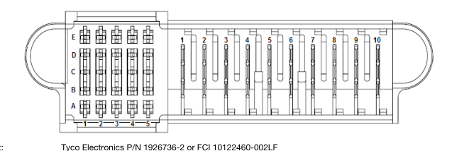
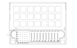
Tyco Electronics P/N 2-1926739-5 or FCI 10108888-R10253SLF (Bel Power Solutions P/N: ZES.00672)
Counter part:
PIN
NAME
DESCRIPTION
Output
6, 7, 8, 9, 10
V1
+12 VDC main output
1, 2, 3, 4, 5
PGND
Power ground (return)
Control Pins
Standby positive output (+3.3 V)
A1, B1, C1, D1, E1 VSB
A2, B2
SGND
Signal ground (return)
C2
NC
Reserved
D2
NC
Reserved
E2
NC
Reserved
Power supply kill (lagging pin)
A3
PS_KILL
B3
NC
Reserved
I2C data signal line
C3
SDA
D3
V1_SENSE_R Main output negative sense
E3
V1_SENSE
Main output positive sense
I2C clock signal line
A4
SCL
Power supply on input (connect to A2/B2 to
B4
PS_ON_L
turn unit on)
C4
ALERT_L
SMB Alert signal output
12 V current share signal (LS)
D4
ISHARE
E4
AC_OK
AC input OK signal
A5
A0
Address 0
B5
NC
Reserved
Power OK signal output (lagging pin)
C5
PW_OK
D5
A1
Address 1
PRESENT_L Power supply present (lagging pin)
E5

Page 18
18
ORDERING PART
ITEM
DESCRIPTION
SOURCE
NUMBER
Bel Power Solutions I2C Utility
Windows XP/Vista/7 compatible GUI to
N/A
program, control and monitor PET Front- Ends (and other I2C units)


Page 19
19
14.1 ADDRESS SELECT
A2
A1
A0
UNIT ADDRESS
EEPROM ADDRESS
0
0
0
0xB0
0xA0
0
0
1
0xB2
0xA2
0
1
0
0xB4
0xA4
0
1
1
0xB6
0xA6
NOTE: A2 = 1 is not implemented.
Table 8. Address Select
14.2 PMBus® COMMANDS
NOTE:
Reference: PMBus® Power System Management Protocol Specification Part II – Command Language Revision 1.1. Commands not included in the table below are Not Implemented. Feature that are To Be Defined (TBD), or Not Implemented are shaded. R = Read-Only; RW = Read/Write; W = Write-Only.
| COMMAND NAME BIT NAME | CODE | BIT | VALUE | ACCESS | DATA BYTES | REMARKS |
| PAGE | 00h | - | RW | 1 | Page 0 applies to + 12 V output Page 1 applies to + 3.3 V output Other Page values are considered invalid and will generate an INVALID_DATA error. | |
| OPERATION | 01h | 1 | ||||
| 7-6 | - | RW | 0b00 = OFF 0b10 = ON (Default) | |||
| 5-0 | 0d | R | Not Implemented | |||
| CLEAR_FAULTS | 03h | - | W | 0 | Clear all bits in all status registers. | |
| CAPABILITY | 19h | R | 1 | |||
| PACKET_ERROR_CHECKING | 7 | 0b1 | Supported | |||
| MAXIMUM_BUS_SPEED | 6-5 | 0b01 | 400 kHz | |||
| SMBALERT# | 4 | 0b1 | Supported | |||
| RESERVED | 3-0 | 0b0000 | Reserved | |||
| VOUT_MODE | 20h | - | R | 1 | ||
| MODE | 7-5 | 0b000 | Linear | |||
| PARAMETER | 4-0 | 0b10111 | N = -9 | |||
| FAN_CONFIG_1_2 | 3Ah | R | 1 | |||
| 7 | 0b1 | Fan1 Installed | ||||
| 6 | 0b0 | Fan1 Commanded in Duty Cycle | ||||
| 5-4 | 0b01 | Fan1 (2) Tachometer Pulses per Revolution | ||||
| 3 | 0b0 | Fan2 Not Installed | ||||
| 2 | 0b0 | Don’t Care | ||||
| 1-0 | 0b00 | Don’t Care | ||||
| FAN_COMMAND_1 | 3Bh | - | RW | 2 | MIN = 0 0% MAX = 100 100% Values outside limits will generate INVALID_DATA error. Write request is executed only if the desired Fan speed is greater than what is required by the PSU. Fan Speed = FAN_COMMAND*21000RPM/100 |

Page 20
20
| COMMAND NAME BIT NAME | CODE | BIT | VALUE | ACCESS | DATA BYTES | REMARKS |
| STATUS_BYTE | 78h | R | 1 | STATUS bits remain set, even if the fault or warning is removed. They are reset by: CLEAR_FAULTS Command AC Recycle PSON Recycle | ||
| BUSY | 7 | 0b0 | Not Implemented | |||
| OFF | 6 | - | ||||
| VOUT_OV | 5 | - | ||||
| IOUT_OC | 4 | - | ||||
| VIN_UV | 3 | - | ||||
| TEMPERATURE | 2 | - | ||||
| CML | 1 | - | ||||
| NONE_OF_THE_ABOVE | 0 | 0b0 | Not Implemented | |||
| STATUS_WORD | 79h | R | 2 | |||
| VOUT | F | - | ||||
| IOUT/POUT | E | - | ||||
| INPUT | D | - | ||||
| MFR | C | - | ||||
| POWER_GOOD# | B | - | ||||
| FANS | A | - | ||||
| OTHER | 9 | - | ||||
| UNKNOWN | 8 | 0b0 | Not Implemented | |||
| STATUS_BYTE | 7-0 | - | See STATUS_BYTE | |||
| STATUS_VOUT | 7Ah | R | 1 | |||
| VOUT_OV_FAULT | 7 | - | Asserts when an OV fault condition is detected on V1 output. SMB Alert Mask = 1 (Default) | |||
| VOUT_OV_WARNING | 6 | 0b0 | Not Implemented | |||
| VOUT_UV_WARNING | 5 | 0b0 | Not Implemented | |||
| VOUT_UV_FAULT | 4 | - | Asserts when an UV fault condition is detected on V1 output. SMB Alert Mask = 1 (Default) | |||
| VOUT_MAX_WARNING | 3 | 0b0 | Not Implemented | |||
| TON_MAX_FAULT | 2 | - | Asserts when V1 output is not in regulation 3s after PSON and AC is applied. SMB Alert Mask = 1 (Default) | |||
| TOFF_MAX_WARNING | 1 | 0b0 | Not Implemented | |||
| PWR_ON_TRACKING_ERROR | 0 | 0b0 | Not Implemented | |||
| STATUS_IOUT | 7Bh | R | 1 | |||
| IOUT_OC_FAULT | 7 | - | Asserts when an OC fault condition is detected on V1 output. SMB Alert Mask = 1 (Default) | |||
| IOUT_OC_FAULT_LV | 6 | 0b0 | Not Implemented | |||
| IOUT_OC_WARNING | 5 | 0b0 | Asserts when an OC warning condition is detected on V1 output. SMB Alert Mask = 0 (Default) | |||
| IOUT_UC_FAULT | 4 | 0b0 | Not Implemented | |||
| ISHARE_FAULT | 3 | 0b0 | Not Implemented | |||
| PIN_LIMITING_MODE | 2 | 0b0 | Not Implemented | |||
| POUT_OP_FAULT | 1 | 0b0 | Not Implemented | |||
| POUT_OP_WARNING | 0 | 0b0 | Not Implemented | |||
| STATUS_INPUT | 7Ch | R | 1 | |||
| VIN_OV_FAULT | 7 | 0b0 | Not Implemented | |||
| VIN_OV_WARNING | 6 | 0b0 | Not Implemented | |||
| VIN_UV_WARNING | 5 | 0b0 | Not Implemented |

Page 21
21
| COMMAND NAME BIT NAME | CODE | BIT | VALUE | ACCESS | DATA BYTES | REMARKS |
| VIN_UV_FAULT | 4 | 0b0 | Not Implemented | |||
| UNIT_OFF_VIN_LOW | 3 | - | Asserts when the PSU is disabled because of low input voltage. SMB Alert Mask = 1 (Default) | |||
| IIN_OC_FAULT | 2 | 0b0 | Not Implemented | |||
| IIN_OC_WARNING | 1 | 0b0 | Not Implemented | |||
| PIN_OP_WARNING | 0 | 0b0 | Not Implemented | |||
| STATUS_TEMPERATURE | 7Dh | R | 1 | |||
| OT_FAULT | 7 | - | Asserts when an OT fault condition is detected. SMB Alert Mask = 1 (Default) | |||
| OT_WARNING | 6 | - | Asserts when an OT warning condition is detected. SMB Alert Mask = 1 (Default) | |||
| UT_WARNING | 5 | 0b0 | Not Implemented | |||
| UT_FAULT | 4 | 0b0 | Not Implemented | |||
| RESERVED | 3-0 | 0b0000 | Reserved | |||
| STATUS_CML | 7Eh | R | 1 | |||
| INVALID_COMMAND | 7 | - | Asserts when the System tries to access unsupported commands, write to supported commands with read-only access, or read supported commands with write-only access. SMB Alert Mask = 0 (Default) | |||
| INVALID_DATA | 6 | - | Asserts when the System tries to write invalid data (including when PEC byte is incorrect) to supported commands with write access. SMB Alert Mask = 0 (Default) | |||
| PEC_FAIL | 5 | - | Asserts when the received PEC byte is incorrect. SMB Alert Mask = 0 (Default) | |||
| MEMORY_FAULT | 4 | 0b0 | Not Implemented | |||
| PROCESSOR_FAULT | 3 | 0b0 | Not Implemented | |||
| RESERVED | 2 | 0b0 | Reserved | |||
| OTHER_COMM_FAULT | 1 | 0b0 | Asserts when the communication between monitoring components inside the PSU is lost. SMB Alert Mask = 0 (Default) | |||
| OTHER_MEMORY_FAULT | 0 | 0b0 | Not Implemented | |||
| STATUS_OTHER | 7Fh | R | 1 | |||
| RESERVED | 7 | 0b0 | Reserved | |||
| RESERVED | 6 | 0b0 | Reserved | |||
| INPUT A FUSE | 5 | 0b0 | Not Implemented | |||
| INPUT B FUSE | 4 | 0b0 | Not Implemented | |||
| INPUT A ORING | 3 | 0b0 | Not Implemented | |||
| INPUT B ORING | 2 | 0b0 | Not Implemented | |||
| OUTPUT ORING | 1 | - | Asserts when a fault is detected on the V1 ORing device. SMB Alert Mask = 0 (Default) | |||
| RESERVED | 0 | 0b0 | Reserved | |||
| STATUS_MFR_SPECIFIC | 80h | R | 1 | |||
| RESERVED | 7 | 0b0 | Reserved | |||
| RESERVED | 6 | 0b0 | Reserved | |||
| RESERVED | 5 | 0b0 | Reserved | |||
| RESERVED | 4 | 0b0 | Reserved | |||
| VSB_UV_FAULT | 3 | - | Asserts when an UV fault condition is detected on Vsb output. SMB_Alert Mask = 0 (Default) | |||
| VSB_OV_FAULT | 2 | - | Asserts when an OV fault condition is detected on Vsb output. SMB_Alert Mask = 0 (Default) |

Page 22
22
| COMMAND NAME BIT NAME | CODE | BIT | VALUE | ACCESS | DATA BYTES | REMARKS |
| PHASE_SHARE_FAULT | 1 | - | Asserts when there is a current imbalance between DCDC Phases. SMB_Alert Mask = 0 (Default) | |||
| HOLDUP_FAULT | 0 | - | Asserts when V1 goes out of regulation if Bulk voltage level is reduced. SMB_Alert Mask = 0 (Default) | |||
| STATUS_FANS_1_2 | 81h | R | 1 | |||
| FAN1_FAULT | 7 | - | Asserts when a Fan fault condition is detected. SMB Alert Mask = 1 (Default) | |||
| FAN2_FAULT | 6 | 0b0 | Not Implemented | |||
| FAN1_WARNING | 5 | 0b0 | Not Implemented | |||
| FAN2_WARNING | 4 | 0b0 | Not Implemented | |||
| FAN1_SPEED_OVERRIDE | 3 | - | Asserts when the Fan is running according to the speed defined by the System. SMB Alert Mask = 0 (Default) | |||
| FAN2_SPEED_OVERRIDE | 2 | 0b0 | Not Implemented | |||
| AIR_FLOW_FAULT | 1 | 0b0 | Not Implemented | |||
| AIR_FLOW_WARNING | 0 | 0b0 | Not Implemented | |||
| READ_VIN | 88h | - | R | 2 | Linear Format, N = -1 | |
| READ_IIN | 89h | - | R | 2 | Linear Format, N = -6 | |
| READ_VOUT | 8Bh | - | R | 2 | Linear Format, N = -9 Refer to Section 8.3.1 of PMBus® Spec Part II Revision 1.1 | |
| READ_IOUT | 8Ch | - | R | 2 | Linear Format, N = -3 | |
| READ_TEMPERATURE_1 | 8Dh | - | R | 2 | Linear Format, N = -2 Inlet Temperature | |
| READ_TEMPERATURE_2 | 8Eh | - | R | 2 | Linear Format, N = -2 Outlet Temperature | |
| READ_TEMPERATURE_3 | 8Fh | - | R | 2 | Linear Format, N = -2 ORing FET Temperature | |
| READ_FAN_SPEED_1 | 90h | - | R | 2 | Linear Format, N = 5 | |
| READ_POUT | 96h | - | R | 2 | Linear Format, N = 1 | |
| READ_PIN | 97h | - | R | 2 | Linear Format, N = 1 | |
| MFR_ID | 99h | - | R | CNT+9 | ID = Bel Power Format: ASCII | |
| MFR_MODEL | 9Ah | - | R | CNT+16 | MODEL = PET1300-12-054xA Format: ASCII | |
| MFR_REVISION | 9Bh | - | R | CNT+3 | REVISION = vvv Format: ASCII | |
| MFR_LOCATION | 9Ch | - | R | 2 | LOCATION = xx Format: ASCII | |
| MFR_DATE | 9Dh | - | R | CNT+4 | DATE = yyww Format: ASCII | |
| MFR_SERIAL | 9Eh | - | R | CNT+18 | SERIAL = xxzzzzzzzzvvvuuuuu Format: ASCII | |
| CALIBRATION_POINTER | C0h | - | RW | 2 | For Bel Power Solutions Use Only | |
| CALIBRATION_DATA | C1h | - | RW | 2 | For Bel Power Solutions Use Only | |
| CALIBRATION_COMMAND | C2h | - | 2 | For Bel Power Solutions Use Only | ||
| RESERVED | F-1 | 0d | R | Reserved | ||
| COMMIT_TO_FLASH | 0 | - | RW | 0 = No Action 1 = Commit RAM to Flash | ||
| READ_VSTBY | C3h | - | R | 2 | For Bel Power Solutions Use Only Same format as READ_VOUT | |
| READ_ISTBY | C4h | - | R | 2 | For Bel Power Solutions Use Only Same format as READ_IOUT | |
| READ_VOUT_INT | C5h | - | R | 2 | For Bel Power Solutions Use Only Same format as READ_VOUT | |
| BOOTLOADER_STATUS_REQUEST | C7h | RW | 2 | For Bel Power Solutions Use Only | ||
| BOOTLOADER_PAGE_DATA | C8h | - | W | - | For Bel Power Solutions Use Only | |
| PRODUCT_ID_NUMBER | C9h | R | 2 | For Bel Power Solutions Use Only |

Page 23
23
| COMMAND NAME BIT NAME | CODE | BIT | VALUE | ACCESS | DATA BYTES | REMARKS |
| Refer to Table 3 | ||||||
| FW_REV | CAh | R | 2 | For Bel Power Solutions Use Only | ||
| SEC_DSP_MAJOR | F-C | - | M = 0 to 9 | |||
| SEC_DSP_MINOR | B-8 | - | m = 0 to 9 i.e: Mm = 25 Revision 2.5 | |||
| PRI_DSP_MAJOR | 7-4 | - | M = 0 to 9 | |||
| PRI_DSP_MINOR | 3-0 | - | m = 0 to 9 i.e: Mm = 13 Revision1.3 | |||
| SEC_CTRL1 | CCh | R | For Bel Power Solutions Use Only | |||
| SEC_CTRL2 | CDh | R | For Bel Power Solutions Use Only | |||
| SEC_STAT | CEh | R | For Bel Power Solutions Use Only | |||
| PRI_STAT | CFh | R | For Bel Power Solutions Use Only | |||
| MFR_SPECIFIC_00 (PSU_CONTROL) | D0h | 2 | ||||
| RESERVED | F-1 | 0d | R | Reserved | ||
| EEPROM_WP | 0 | - | RW | EEP Write-Protect (WP) Control 0 = Enable WP (Default) 1 = Disable WP | ||
| MFR_SPECIFIC_05 (FW_VERSION) | D5h | - | R | 8 | Format: xx.xx.xx (e.g. 01.02.01). The length is fixed at 8 Ascii characters. Each field will be an Ascii value stored in one byte. * For example: aa.bb.cc, where aa is development stage (P0, P1 ... A0); bb is primary mcu firmware revision (00 ~ 99); cc is secondary mcu firmware revision (00 ~ 99). NO BYTE COUNT | |
| MFR_SPECIFIC_09 (SMB_ALERT_MASKING) | D9h | - | RW | 7 | Refer to Table 4 NO BYTE COUNT |
Table 9. PMBus® Commands
NUCLEAR AND MEDICAL APPLICATIONS - Products are not designed or intended for use as critical components in life support systems, equipment used in hazardous environments, or nuclear control systems. TECHNICAL REVISIONS - The appearance of products, including safety agency certifications pictured on labels, may change depending on the date manufactured. Specifications are subject to change without notice.