

 Download PDF
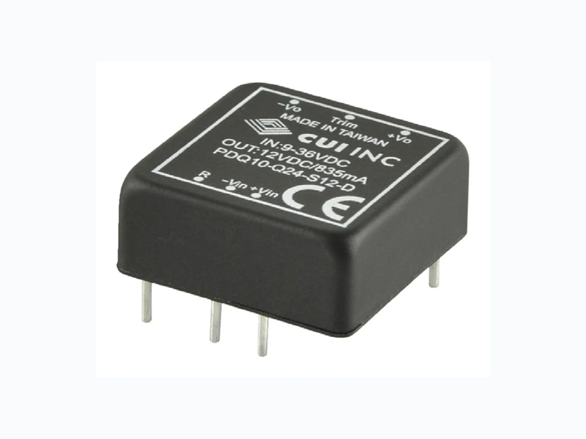
PDQ10-D CUI
Document overview
- PDF pages: 9
Technical content
Page 1
SERIES: PDQ10-D │ DESCRIPTION: DC-DC CONVERTER
FEATURES
- up to 10 W isolated output
- industry standard 1” x 1” package
- 4:1 input range
- single/dual regulated output
- over voltage, input under voltage lockout, and short circuit protections
- 1,500 Vdc isolation voltage
- five-sided shielded case
- remote on/off control
- output trim
- -40 to 105°C temperature range
- efficiency up to 86%
MODEL
input
output
voltage
voltage
typ range
min
(Vdc)
(Vdc)
(Vdc)
(mA)
PDQ10-Q24-S3-D
24 9~36
3.3
0
PDQ10-Q24-S5-D
24 9~36
5
0
PDQ10-Q24-S12-D
24 9~36
12
0
PDQ10-Q24-S15-D
24 9~36
15
0
PDQ10-Q24-D5-D
24 9~36
±5
0
PDQ10-Q24-D12-D
24 9~36
±12
0
PDQ10-Q24-D15-D
24 9~36
±15
0
PDQ10-Q48-S3-D
48 18~75
3.3
0
PDQ10-Q48-S5-D
48 18~75
5
0
PDQ10-Q48-S12-D
48 18~75
12
0
PDQ10-Q48-S15-D
48 18~75
15
0
PDQ10-Q48-D5-D
48 18~75
±5
0
PDQ10-Q48-D12-D
48 18~75
±12
0
PDQ10-Q48-D15-D
48 18~75
±15
0
date 07/12/2016 page 1 of 9
output
output
ripple efficiency
current
power & noise1
max
max
max
typ
(mA)
(W) (mVp-p)
(%)
2500
8.25
75
81
2000
10
75
84
835
10 100
86
666
10 100
86
±1000
10
75
84
±416
10 100
86
±333
10 100
86
2500
8.25
75
82
2000
10
75
84
835
10 100
86
666
10 100
86
±1000
10
75
84
±416
10 100
86
±333
10 100
86
- At full load, nominal input, 20 MHz bandwidth oscilloscope, with 10 µF tantalum and 1 µF ceramic capacitors on the output. Notes: 2. All specifications are measured at Ta=25°C, nominal input voltage, and rated output load unless otherwise specified.
PART NUMBER KEY
PDQ10 - QXX - X XX - D

Packaging Style:
S = single D = dual
Page 2
date 07/12/2016 │ page 2 of 9
INPUT
parameter
conditions/description
min
typ
max
units
24 Vdc input models
9
24
36
Vdc
operating input voltage
48 Vdc input models
18
48
75
Vdc
for maximum of 100 ms
surge voltage
24 Vdc input models
50
Vdc
48 Vdc input models
100
Vdc
24 Vdc input models
1.4
A
current
48 Vdc input models
0.7
A
24 Vdc input models, power up
8.8
Vdc
24 Vdc input models, power down
8.0
Vdc
under voltage shutdown
48 Vdc input models, power up
17
Vdc
48 Vdc input models, power down
16
Vdc
turn on (3.5~36 Vdc or open circuit)
remote on/off1
turn off (<1.2 Vdc)
filter
LC type
input reverse polarity protection no
3 A time delay fuse for 24 Vdc input models (recommended)
input fuse
1.5 A time delay fuse for 48 Vdc input models (recommended)
Notes: 1. CMOS or open collector TTL, reference to –Vin.
OUTPUT
parameter
conditions/description
min
typ
max
units
3.3 Vdc output models
3,300
μF
5 Vdc output models
2,200
μF
12 Vdc output models
1,000
μF
maximum capacitive load
15 Vdc output models
680
μF
±5 Vdc output models
1,200
μF
±12 Vdc output models
470
μF
±15 Vdc output models
330
μF
voltage accuracy
±1.5
%
line regulation
from high line to low line
±0.5
%
from 100% load to minimum load
load regulation
single output models
±0.5
%
dual output models
±1
%
voltage balance
dual output models
±1
%
load cross variation 25%/100% (dual output
cross regulation
±5
%
models)
turn-on delay time, from input from Vin, min to 10% Vo
2
ms
turn-on delay time, from
from Von/off to 10% Vo
2
ms
on/off control rise time
from 10% Vo to 90% Vo
1.5
ms
adjustability2
see application notes
±10
%
switching frequency
at nominal Vin, full load
280
kHz
75%-100% step load change
dynamic load response
error band (Vout)
5
%
recovery time
500
µs
temperature coefficient
±0.03
%/°C
Note: 2. For single output models only.
Page 3
PROTECTIONS
parameter
conditions/description zener or TVS clamp 3.3 Vdc output models
over voltage protection
5 Vdc output models (single and dual) 12 Vdc output models (single and dual) 15 Vdc output models (single and dual)
over current protection short circuit protection
continuous, automatic recovery
SAFETY AND COMPLIANCE
parameter
conditions/description
isolation voltage
input to output for 1 minute
isolation resistance
input to output
isolation capacitance
input to output EN 55022 Class A & Class B (external circuit
conducted emissions
required, see Figure 3)
MTBF
as per MIL-HDBK-217F, GB
RoHS
2011/65/EU
ENVIRONMENTAL
parameter
conditions/description
operating temperature
see derating curves
storage temperature operating humidity
non-condensing
SOLDERABILITY
parameter
conditions/description
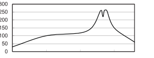
wave soldering
see wave soldering profile
Notes: 1. Soldering materials: Sn/Cu/Ni 2. Ramp up rate during preheat: 1.4°C/s (from 50°C to 100°C) 3. Soaking temperature: 0.5°C/s (from 100°C to 130°C), 60±20 seconds 4. Peak temperature: 260°C, above 250°C for 3~6 seconds 5. Ramp down rate during cooling: -10°C/s (from 260°C to 150°C)
date 07/12/2016 │ page 3 of 9
min
typ
max
units
3.9
Vdc
6.2
Vdc
15
Vdc
18
Vdc
120
%
min
typ
max
units
1,500
Vdc
1,000
MΩ
1,000
pF
1,300,000
hours
min
typ
max
units
-40
105
°C
-55
125
°C
95
%
min
typ
max
units 260
°C
Time (Seconds)
Page 4
date 07/12/2016 │ page 4 of 9
MECHANICAL
parameter
conditions/description
min
typ
max
units
1.00 x 1.00 x 0.4 [25.4 x 25.4 x 10.2 mm]
dimensions
inches
black coated copper with non-conductive base
case material weight
18
g
MECHANICAL DRAWING
units: inches [mm]
0.200
tolerance: X.XX ±0.02 [±0.5]
[5.08]
X.XXX ±0.010 [±0.25]
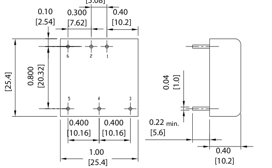
pin diameter tolerance: ±0.004[±0.1]
| PIN CONNECTIONS | ||
| PIN | Function | |
| Single | Dual | |
| 1 | +Vin | +Vin |
| 2 | -Vin | -Vin |
| 3 | +Vout | +Vout |
| 4 | Trim | Common |
| 5 | -Vout | -Vout |
| 6 | Remote | Remote |
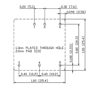
Recommended PCB Layout
Top View
Page 5
date 07/12/2016 │ page 5 of 9
DERATING CURVE
Temperature Derating Curve
(Natural Convention)
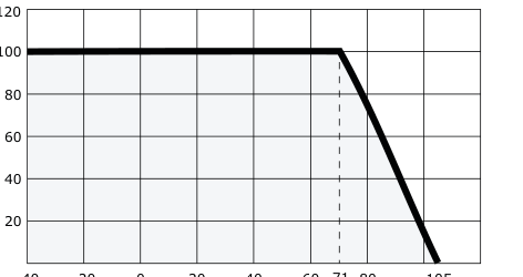
71
-40 -20 0 20 40 60 80 105
Ambient Temperature (°C)
EFFICIENCY CURVES
PDQ10-Q24-S3-D Efficiency Curve (Efficiency vs. Line Voltage and Load Current)
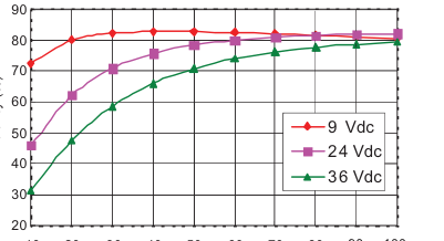
70 80 90 100
10 20 30 40 50 60
Load Current (%)
PDQ10-Q24-S15-D Efficiency Curve (Efficiency vs. Line Voltage and Load Current)
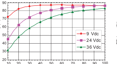
Load Current (%)
PDQ10-Q24-S12-D Efficiency Curve (Efficiency vs. Line Voltage and Load Current)
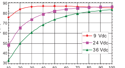
100
10 20 30 40 50 60 70 80 90
Load Current (%)
PDQ10-Q24-D5-D Efficiency Curve (Efficiency vs. Line Voltage and Load Current)
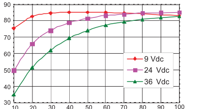
Load Current (%)
Page 6
EFFICIENCY CURVES (CONTINUED)
PDQ10-Q24-D15-D Efficiency Curve (Efficiency vs. Line Voltage and Load Current)
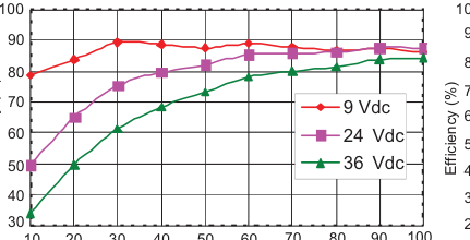
90 100
10 20 30 40 50 60 70 80
Load Current (%)
PDQ10-Q48-S12-D Efficiency Curve (Efficiency vs. Line Voltage and Load Current)
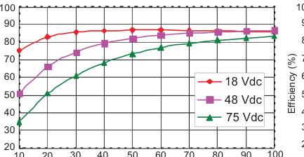
10 20 30 40 50 60 70 80
Load Current (%)
PDQ10-Q48-D5-D Efficiency Curve (Efficiency vs. Line Voltage and Load Current)
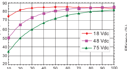
Load Current (%)
date 07/12/2016 │ page 6 of 9
PDQ10-Q48-S3-D Efficiency Curve (Efficiency vs. Line Voltage and Load Current)
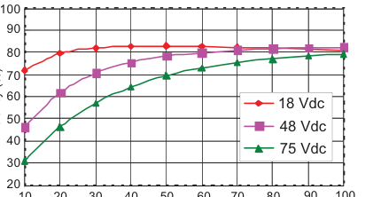
100
10 20 30 40 50 60 70 80 90
Load Current (%)
PDQ10-Q48-S15-D Efficiency Curve (Efficiency vs. Line Voltage and Load Current)
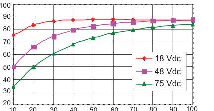
10 20 30 40 50 60
Load Current (%)
PDQ10-Q48-D15-D Efficiency Curve (Efficiency vs. Line Voltage and Load Current)
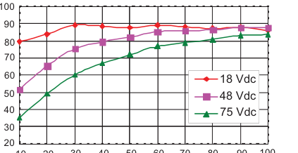
Load Current (%)
Page 7
TEST CONFIGURATIONS
Input Ripple Current & Output Noise
Figure 1 Measuring Input Ripple Current
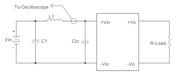
Table 1
| L1 | 1 µH |
| C1 | 6.8 µF ceramic capacitor |
| Cin | none |
EMC RECOMMENDED CIRCUIT
Test Condition Input Voltage: Nominal Output Load: Full Load
date 07/12/2016 │ page 7 of 9
Figure 2 Measuring Output Ripple And Noise
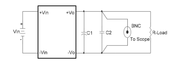
Table 2
| C1 | 10 µF tantalum capacitor |
| C2 | 1 µF ceramic capacitor |
Figure 3 Conducted Emissions Test Circuit
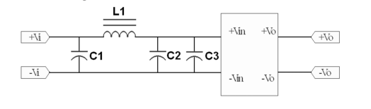
Table 3
Table 4
| EN55022 Class A Recommended External Circuit Components | ||||
| Input Voltage (Vdc) | C1 | C2 | C3 | L1 |
| 24 | NC | 10 µF / 50 V | 10 µF / 50 V | short |
| 48 | NC | 4.7 µF / 100 V | 4.7 µF / 100 V | short |
| EN55022 Class B Recommended External Circuit Components | ||||
| Input Voltage (Vdc) | C1 | C2 | C3 | L1 |
| 24 | 10 µF / 50 V | NC | 10 µF / 50 V | 3.3 µH |
| 48 | 4.7 µF / 100 V | NC | 4.7 µF / 100 V | 3.3 µH |
Page 8
date 07/12/2016 │ page 8 of 9
APPLICATION NOTES
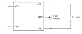
Output Voltage Trimming The output voltage can be adjusted (single outputs only) by using the trim pin and the use of either an external trim pot or the use of a single fixed resistor (see Figures below). If the trim function is not needed, leave the trim pin open.
Figure 5 Trim Adjustments To Increase
Figure 4 Trim Adjustments Using
Figure 6 Trim Adjustments To Decrease
Output Voltage Using A Fixed Resistor
A Trimpot
Output Voltage Using A Fixed Resistor
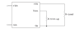
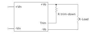
Formula for Trim Resistor
Vr R1 (R2 R3)
R
) Rt (k )
( trim up
Vo V ) R2
(
| Output Voltage (Vdc) | R1 (kΩ) | R2 (kΩ) | R3 (kΩ) | Rt (kΩ) | Vr (V) |
| 3.3 | 2.74 | 1.8 | 0.27 | 9.1 | 1.24 |
| 5 | 2.32 | 2.32 | 0 | 8.2 | 2.5 |
| 12 | 6.8 | 2.4 | 2.32 | 22 | 2.5 |
| 15 | 8.06 | 2.4 | 3.9 | 27 | 2.5 |
o, nom
Vr R 1
R
R1 (
)1 Rt (k )
trim down
Table 5
V Vo) R2 ( o, nom
Note: Rtrim-up is the external resistor in kΩ Rtrim-down is the external resistor in kΩ VO, nom is the nominal output voltage VO is the desired output voltage R1, R2, R3, Rt, and Vr are internal (see Table 5).
Page 9
date 07/12/2016 │ page 9 of 9
REVISION HISTORY
| rev. | description | date |
|---|---|---|
| 1.0 | initial release | 07/12/2016 |
The revision history provided is for informational purposes only and is believed to be accurate.
Headquarters 20050 SW 112th Ave.
Fax 503.612.2383
Tualatin, OR 97062 800.275.4899
techsupport@cui.com
CUI offers a two (2) year limited warranty. Complete warranty information is listed on our website.
CUI reserves the right to make changes to the product at any time without notice. Information provided by CUI is believed to be accurate and reliable. However, no responsibility is assumed by CUI for its use, nor for any infringements of patents or other rights of third parties which may result from its use.
CUI products are not authorized or warranted for use as critical components in equipment that requires an extremely high level of reliability. A critical component is any component of a life support device or system whose failure to perform can be reasonably expected to cause the failure of the life support device or system, or to affect its safety or effectiveness.