
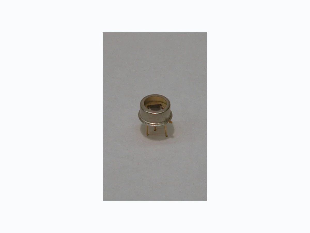
PDB-C201 ETC2
Document overview
- Manufacturer or author: Provided By www.digicamel.com(FREE DATASHEET DOWNLOAD SITE)
- PDF pages: 1
Technical content
FEATURES DESCRIPTION APPLICATIONS
- Low capacitance
- Blue enhanced
- High speed
- Low dark current SYMBOL PARAMETER MIN MAX UNITS VBR Reverse Voltage 100 V TSTG Storage Temperature -55 +150 °C TO Operating Temperature -40 +125 °C TS Soldering Temperature* +240 °C SYMBOL CHARACTERISTIC TEST CONDITIONS MIN TYP MAX UNITS ISC Short Circuit Current H = 100 fc, 2850 K 50 75 µA ID Dark Current VR = 5V 0.5 2.0 nA RSH Shunt Resistance VR = 10 mV 250 500 M Ω CJ Junction Capacitance VR =10 V, f = 1 MHz 15 pF lrange Spectral Application Range Spot Scan 350 1100 nm VBR Breakdown Voltage I = 10 μA 50 75 V NEP Noise Equivalent Power VR = 0V @ l=Peak 1X10 -14 W/ √ Hz RL = 50 Ω,VR = 0 V 190 tr Response Time** RL = 50 Ω,VR = 10 V 13 nS SPECTRAL RESPONSE 0.00 0.10 0.20 0.30 0.40 0.50 0.60 0.70 0.80 250 300 350 400 450 500 550 600 650 700 750 800 850 900 950 1000 1050 1100 1150Wavelength (nm) Responsivity (A/W) PDB-C201 PACKAGE DIMENSIONS INCH [mm] TO-46 PACKAGE The PDB-C201 is a blue enhanced Bi-Cell silicon photodiode used for nulling, centering, or measuring small positional changes packaged in a hermetic TO-5 metal package.
- Emitter Alignment
- Position sensing
- Medical and Industrial * 1/16 inch from case for 3 seconds max. ELECTRO-OPTICAL CHARACTERISTICS RATING (TA)= 23°C UNLESS OTHERWISE NOTED **Response time of 10% to 90% is specified at 660nm wavelength light. Information in this technical datasheet is believed to be correct and reliable. However, no responsibility is assumed for possible inaccuracies or omission. Specifications are subject to change without notice. ABSOLUTE MAXIMUM RATING (TA)= 23°C UNLESS OTHERWISE NOTED CHIP DIMENSIONS INCH [mm] PACKAGE DIMENSIONS INCH [mm] CHIP DIMENSIONS INCH [mm] TO-5 PACKAGE .150 [3.81] SQUARE 2X .050 [1.27] ACTIVE AREA 2X .100 [2.54] ACTIVE AREA .004 [0.10] GAP ANODE CELL #1 CELL 1 CELL 2
3 ANODE CELL #2
CASE GROUND & COMMON CATHODE SCHEMATIC 72° VIEWING ANGLE Ø.245 [6.22] Ø.255 [6.48] Ø.320 [8.13] Ø.330 [8.38] 3X .50 [12.7] MIN 3X Ø.018 [0.46] .010 [0.25] MAX GLASS ABOVE CAP TOP EDGE .075 [1.91] .168 [4.27] 45° Ø.200 [5.08] PIN CIRCLE Ø .362 [9.19] Ø .357 [9.07] Blue Enhanced Bi-Cell Silicon Photodiode www.lasercomponents.com Issue: 08/06 / V1 / HW / api/si-pin/bi-cells/ pdb-c201.pdf Germany and other countries: LASER COMPONENTS GmbH, Phone: +49 8142 2864 0, Fax: +49 8142 2864 11, info@lasercomponents.com Great Britain: LASER COMPONENTS (UK) Ltd., Phone: +44 1245 491 499, Fax: +44 1245 491 801, info@lasercomponents.co.uk