
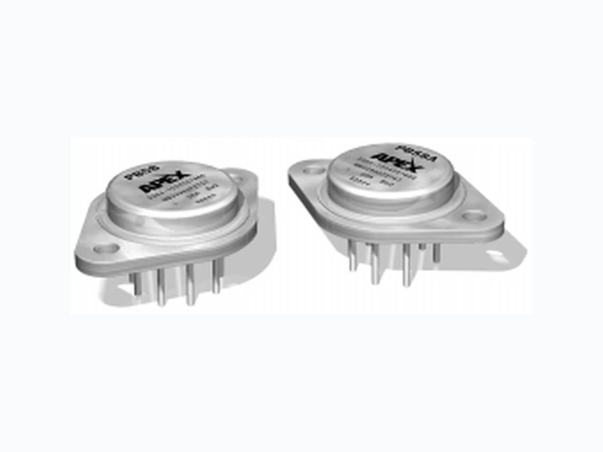
PB58 ETC
Document overview
- Manufacturer or author: Provided By www.digicamel.com(FREE DATASHEET DOWNLOAD SITE)
- PDF pages: 4
Technical content
APEX MICROTECHNOLOGY CORPORATION • TELEPHONE (520) 690-8600 • FAX (520) 888-3329 • ORDERS (520) 690-8601 • EMAIL prodlit@apexmicrotech.com
FEATURES
- WIDE SUPPLY RANGE — ±15V to ±150V
- HIGH OUTPUT CURRENT — 1.5A Continuous (PB58) 2.0A Continuous (PB58A)
- VOLTAGE AND CURRENT GAIN
- HIGH SLEW — 50V/ µs Minimum (PB58) 75V/µs Minimum (PB58A)
- PROGRAMMABLE OUTPUT CURRENT LIMIT
- HIGH POWER BANDWIDTH — 320 kHz Minimum
- LOW QUIESCENT CURRENT — 12mA Typical
- EVALUATION KIT — See EK50
APPLICATIONS
- HIGH VOLTAGE INSTRUMENTATION
- Electrostatic TRANSDUCERS & DEFLECTION
- Programmable Power Supplies Up to 280V p-p
DESCRIPTION
The PB58 is a high voltage, high current amplifier designed to provide voltage and current gain for a small signal, general purpose op amp. Including the power booster within the feed- back loop of the driver amplifier results in a composite amplifier with the accuracy of the driver and the extended output voltage range and current capability of the booster. The PB58 can also be used without a driver in some applications, requiring only an external current limit resistor to function properly. The output stage utilizes complementary MOSFETs, provid- ing symmetrical output impedance and eliminating second breakdown limitations imposed by Bipolar Transistors. Internal feedback and gainset resistors are provided for a pin-strapable gain of 3. Additional gain can be achieved with a single external resistor. Compensation is not required for most driver/gain configurations, but can be accomplished with a single external capacitor. Enormous flexibility is provided through the choice of driver amplifier, current limit, supply voltage, voltage gain, and compensation. This hybrid circuit utilizes a beryllia (BeO) substrate, thick film resistors, ceramic capacitors and semiconductor chips to maxi- mize reliability, minimize size and give top performance. Ultrasonically bonded aluminum wires provide reliable inter- connections at all operating temperatures. The 8-pin TO-3 package is electrically isolated and hermetically sealed using one-shot resistance welding. The use of compressible isolation washers voids the warranty. TYPICAL APPLICATION Figure 1. Inverting composite amplifier. OP AMP PB58 C F R F VIN R I +15V –15V IN COM +Vs –Vs R CL OUT CC R G R L 6 7 TOP VIEW CL+Vs IN COM –Vs GAIN R G COMP CC OUT R CL EQUIVALENT SCHEMATIC EXTERNAL CONNECTIONS IN GAIN COM COMP Q5Q6 Q10Q9 +Vs OUT CL –Vs Q11 6.2K 50K 3.1K HTTP://WWW.APEXMICROTECH.COM (800) 546-APEX (800) 546-2739MICROTECHNOLOGY POWER BOOSTER AMPLIFIERS PB58 • PB58A
APEX MICROTECHNOLOGY CORPORATION • 5980 NORTH SHANNON ROAD • TUCSON, ARIZONA 85741 • USA • APPLICATIONS HOTLINE: 1 (800) 546-2739 ABSOLUTE MAXIMUM RATINGS SPECIFICATIONSPB58 • PB58A SUPPLY VOLTAGE, +V S to –VS 300V OUTPUT CURRENT, within SOA 2.0A POWER DISSIPATION, internal at T C = 25°C 1 83W INPUT VOLTAGE, referred to COM ±15V TEMPERATURE, pin solder—10 sec max 300 °C TEMPERATURE, junction1 175°C TEMPERATURE, storage –65 to +150 °C OPERATING TEMPERATURE RANGE, case –55 to +125 °C SPECIFICATIONS PB58 ABSOLUTE MAXIMUM RATINGS PARAMETER TEST CONDITIONS 2 MIN TYP MAX MIN TYP MAX UNITS INPUT OFFSET VOLTAGE, initial ±.75 ±1.75 * ±1.0 V OFFSET VOLTAGE, vs. temperature Full temperature range INPUT IMPEDANCE, DC 25 50 * * k Ω INPUT CAPACITANCE 3 * pF CLOSED LOOP GAIN RANGE 3 10 25 * * * V/V GAIN ACCURACY, internal Rg, Rf A GAIN ACCURACY, external Rf A V = 10 ±15 ±25 * * % PHASE SHIFT f = 10kHz, AV CL = 10, CC = 22pF 10 * ° f = 200kHz, AVCL = 10, CC = 22pF 60 * ° OUTPUT VOLTAGE SWING Io = 1.5A (PB58), 2A (PB58A) V S–11 V S –8 V S–15 V S–11 V VOLTAGE SWING Io = 1A V S–10 V S –7 * * V VOLTAGE SWING Io = .1A V S–8 V S –5 * * V CURRENT, continuous 1.5 2.0 A SLEW RATE Full temperature range 50 100 75 * V/ µs CAPACITIVE LOAD Full temperature range 2200 * pF SETTLING TIME to .1% R L = 100Ω , 2V step 2 * µs POWER BANDWIDTH V C = 100 Vpp 160 320 240 * kHz SMALL SIGNAL BANDWIDTH C C = 22pF, AV = 25, Vcc = ±100 100 * kHz SMALL SIGNAL BANDWIDTH C C = 22pF, AV = 3, Vcc = ±30 1 * MHz POWER SUPPLY VOLTAGE, ±V S
4 Full temperature range ±156 ±60 ±150 * * * V
CURRENT, quiescent V S = ±15 11 * mA VS = ±60 12 * mA VS = ±150 14 18 * * mA THERMAL RESISTANCE, AC junction to case 5 Full temp. range, f > 60Hz 1.2 1.3 * * °C/W RESISTANCE, DC junction to case Full temp. range, f < 60Hz 1.6 1.8 * * °C/W RESISTANCE, junction to air Full temperature range 30 * °C/W TEMPERATURE RANGE, case Meets full range specifications –25 25 85 * * * °C NOTES: * The specification of PB58A is identical to the specification for PB58 in applicable column to the left. 1. Long term operation at the maximum junction temperature will result in reduced product life. Derate internal power dissipation to achieve high MTTF (Mean Time to Failure). 2. The power supply voltage specified under typical (TYP) applies, TC = 25°C unless otherwise noted. 3. Guaranteed by design but not tested. 4. +V S and –VS denote the positive and negative supply rail respectively. 5. Rating applies if the output current alternates between both output transistors at a rate faster than 60Hz. 6. +V S/–VS must be at least 15V above/below COM. PB58A The PB58 is constructed from MOSFET transistors. ESD handling procedures must be observed. The internal substrate contains beryllia (BeO). Do not break the seal. If accidentally broken, do not crush, machine, or subject to temperatures in excess of 850°C to avoid generating toxic fumes. CAUTION
APEX MICROTECHNOLOGY CORPORATION • TELEPHONE (520) 690-8600 • FAX (520) 888-3329 • ORDERS (520) 690-8601 • EMAIL prodlit@apexmicrotech.com TYPICAL PERFORMANCE GRAPHS PB58 • PB58A –25 0 25 50 75 100 POWER DERATING INTERNAL POWER DISSIPATION, P(W) –25 25 125 1.5 CURRENT LIMIT SLEW RATE, SR (V/ s) 100 10M FREQUENCY, F (Hz) SMALL SIGNAL RESPONSE OPEN LOOP GAIN, A (dB) 1K 10K 10M –10 SMALL SIGNAL RESPONSE 1K 10K 10M FREQUENCY, F (Hz) –180 100K 1M 10M FREQUENCY, F (Hz) 300 POWER RESPONSE OUTPUT VOLTAGE, V (V ) 100 200 TIME, t (µs) -80 PULSE RESPONSE 300 3K 30K FREQUENCY, F (Hz) .001 HARMONIC DISTORTION DISTORTION, THD (%) .01 .03 –25 75 CASE TEMPERATURE, T (°C) QUIESCENT CURRENT 10002 5 INPUT OFFSET VOLTAGE INPUT OFFSET VOLTAGE, V (V) .01 .05 2 OUTPUT CURRENT, I (A) OUTPUT VOLTAGE SWING VOLTAGE DROP FROM SUPPLY, V — V (V)S O 300K 3M 1K .003 SLEW RATE VS. TEMP. 300 400 100 200 0 50 75 100 SMALL SIGNAL RESPONSE 100K 1 1.5 -1.5 1K 10K 100K 1M 125 100K 1M FREQUENCY, F (Hz) CLOSED LOOP GAIN, A (dB) CURRENT LIMIT, I (A)LIM 50 125 -.5 OS –135 –90 –45 10K CASE TEMPERATURE, T ( °C)C CASE TEMPERATURE, T ( °C)C OPEN LOOP PHASE, (°) ϕ –180 –135 –90 –45 CLOSED LOOP PHASE, (°)ϕ AV = 10CL AV = 3CL AV = 25CL AV = 25CL AV = 10CL AV = 3CL O V +O V -O QUIESCENT CURRENT, I (mA)Q C Vs = –100V Vs = –30V CASE TEMPERATURE, T (°C)C –25 75 1000 25 50 125 Vs = –150V –25 75 CASE TEMPERATURE, T (°C) 1000 25 50 125 C µ Q DRIVER = TL070 V = –60V V = 95V S OP P 100 R = .47 CL Ω R = .68CL Ω R = 1.5CL Ω C = 22pFC C = 22pFC PP 2345 678 -60 -40 -20 80OUTPUT VOLTAGE, V (V)Q R = 35 L Ω R = 1K L Ω -SLEW +SLEW
Mechanical Data” section of the handbook. NOTE: The output stage is protected against transient flyback. nal fast-recovery diodes should be used. are gain, stability, slew rate, and output swing of the driver. driver, but makes stability more difficult to achieve. is equal to the composite gain divided by the booster gain.
- Operate the booster in the lowest practical gain.
- Operate the driver amplifier in the highest practical effec-
- Keep gain-bandwidth product of the driver lower than the
closed loop bandwidth of the booster.
- Minimize phase shift within the loop.
optimum square wave response with the op amp drivers listed. Table 1: Typical values for case where op amp effective gain = 1. Figure 2. Non-inverting composite amplifier. equal to the booster slew rate. when calculating maximum available driver swing. This data sheet has been carefully checked and is believed to be reliable, however, no responsibility is assumed for possible inaccuracies or omissions. All specifications are subject to change without notice. PB58U REV. H JANUARY 1998 © 1998 Apex Microtechnology Corp.