
PAT VISHAY
Document overview
- Manufacturer or author: Provided By www.digicamel.com(free datasheet download site)
- PDF pages: 3
Technical content
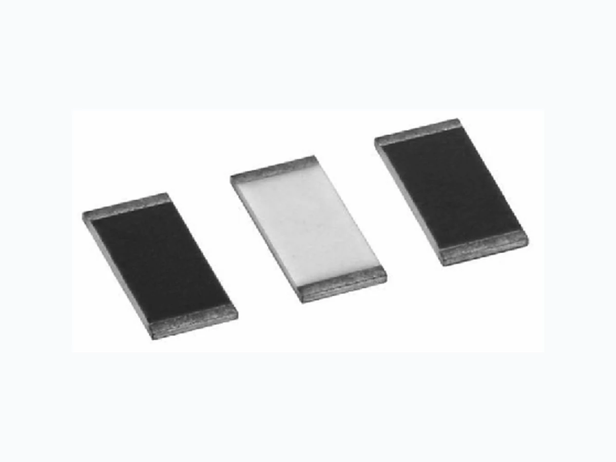
Document Number: 60024 For tec hnical questions, contact: thinfilm@vishay.com www.vishay.com Revision: 25-Aug-10 81 Precision Automotive Thin Film Chip Resistors, AEC-Q200 Qualified, 2 kV ESD Rating PAT Vishay Thin Film These chip resistors are available in wraparound terminations styles in 8 case sizes. They incorporate self passivated enhanced tantalum nitride resistor film to give superior performance on moistu re resistance, electrostatic discharge, voltage coefficient, power handling and resistance stability. The terminations consist of an adhesion layer, a leach resistant nickel barrier, and solder coating (lead (Pb)-free). This produ ct will out-perform all requirements of AEC-Q200. CONSTRUCTION
FEATURES
- Resistance range: 10 Ω to 3 MΩ
- AEC-Q200 qualified
- AEC-Q200 ESD rated class 1C (2 kV)
- Laser trimmed to any value
- Moisture resistant to MIL-STD-202, method 202
- Tantalum nitride resistor film on high purity alumina substrate
- 100 % visual inspected per MIL-PRF-55342
- Laser-trimmed tolerances to ± 0.1 %
- Load life stability < 0.05 % at 1000 h at 70 °C
- Very low noise and voltage coefficient (< - 30 dB, < 0.1 ppm/V)
- Compliant to RoHS directive 2002/95/EC TYPICAL PERFORMANCE Adhesion Layer High Purity Alumina Substrate Nickel Barrier Solder Coating Passivation T antalum Nitride Resistive Film ABSOLUTE TCR 25 TOL. 0.1 STANDARD ELECTRICAL SPECIFICATIONS TEST SPECIFICATIONS CONDITIONS Material Tantalum nitride - Resistance Range 10 Ω to 3 MΩ - TCR: Absolute ± 25 ppm/°C to ± 100 ppm/°C - 55 °C to + 125 °C Tolerance: Absolute ± 0.1 % to ± 1.0 % + 25 °C Stability: Absolute ± 0.05 % 2000 h at 70 °C rated power Stability: Ratio Not applicable - Voltage Coefficient Less than 0.1 ppm/V - Working Voltage 75 V to 200 V - Operating Temperature Range - 55 °C to + 150 °C - Storage Temperature Range - 55 °C to + 150 °C - Noise < - 30 dB - Shelf Life Stability: Absolute 100 ppm 1 year at 25 °C COMPONENT RATINGS CASE SIZE POWER RATING (mW) WORKIN G VOLTAGE (V) RESISTANCE RANGE ( Ω) 0402 50 75 20 to 35K 0603 150 75 10 to 80K 0805 200 100 10 to 301K 1206 400 200 10 to 1M 1505 400 150 10 to 1M 2208 750 150 10 to 1.75M 2010 800 200 10 to 2M 2512 1000 200 10 to 3M ** Please see document “Vishay Material Category Policy”: www.vishay.com/doc?99902
www.vishay.com For technical questions, contact: thinfilm@vishay.com Document Number: 60024 PAT Vishay Thin Film Precision Automotive Thin Film Chip Resistors, AEC-Q200 Qualified, 2 kV ESD Rating Note (1) Preferred packaging code DIMENSIONS in inches CASE SIZE L W T D E ENVIRONMENTAL TESTS (Vishay Performance vs. AEC-Q200 Requirements) ENVIRONMENTAL TEST CONDITIONS LIMITS PER AEC-Q200 TYPICAL VISHAY PERFORMANCE Resistance Temperature Characteristic - 55 °C to + 125 °C ± 50 ppm/°C ± 35 ppm/°C Max. Ambient Temp. at Rated Wattage + 70 °C + 70 °C Max. Ambient Temp. at Power Derating + 150 °C + 150 °C High Temperature Storage ΔR MIL-STD-202, 108, 1000 h at 125 °C ± 0.1 % + 0.016 % Temperature Cycling ΔR JESD22, JA-104, 1000 cycles, - 55 °C to + 125 °C ± 0.15 % + 0.013 % Moisture Resistance ΔR MIL-STD-202, 106 ± 0.20 % + 0.0010 % Biased Humidity ΔR MIL-STD-202, 103, 1000 h at 85 °C, 85 % RH, 10 % P ± 0.10 % + 0.0297 % Life ΔR MIL-STD-202, 108 at 125 °C, 1000 h ± 0.1 % + 0.0220 % Mechanical Shock ΔR MIL-STD-202, method 213, condition C ± 0.1 % + 0.0130 % Vibration ΔR MIL-STD-202 method 204, 10 Hz to 2 kHz ± 0.1 % + 0.0030 % Resistance to Soldering Heat ΔR MIL-STD-202, 204, condition B ± 0.10 % + 0.0150 % Electrostatic Discharge ΔR AEC-Q200-002 at 2 kV, human body ± 0.10 % - 0.032 % Solderability Visual J-STD-002, method B and B1 95 % Acceptable Terminal Strength ΔR AEC-Q200-006 at 1 kg for 60 s ± 0.10 % + 0.012 % Flame Retardance Visual AEC-Q200-001 para 4.0 Acceptable GLOBAL PART NUMBER INFORMATION New Global Part Numbering: PAT1206E1002BST1 GLOBAL MODEL CASE SIZE TCR CHARACTERISTIC RESISTANCE TOLERANCE TERMINATION PACKAGING PAT 0402 0603 0805 1206 1505 2010 2208 2512 E = ± 25 ppm/°C H = ± 50 ppm/°C K = ± 100 ppm/°C The first 3 digits are significant figures and the last digit specifies the number of zeros to follow. “R” designates the decimal point. Example: 10R0 = 10 Ω 1000 = 100 Ω 1002 = 10 kΩ B = ± 0.1 % D = ± 0.5 % F = ± 1.0 % G = ± 2.0 % J = ± 5.0 % S = Wraparound lead (Pb)-free solder w/nickel barrier TAPE AND REEL T1 = 1000 min., 1000 mult (1) TF = Full reel TS = 100 min., 1 mult D L E TW L DT 06E1 02B 01 ST 1TPA 2
Document Number: 91000 www.vishay.com Revision: 18-Jul-08 1 Disclaimer Legal Disclaimer Notice Vishay All product specifications and data are subject to change without notice. Vishay Intertechnology, Inc., its affiliates, agents, and employees, and all persons acting on its or their behalf (collectively, “Vishay”), disclaim any and all liability for any errors, inaccuracies or incompleteness contained herein or in any other disclosure relating to any product. Vishay disclaims any and all li ability arising out of the use or application of any product described herein or of any information provided herein to the maximum extent permit ted by law. The product specifications do not expand or otherwise modify Vishay’s terms and conditions of purcha se, including but not limited to the warranty expressed therein, which apply to these products. No license, express or implied, by estoppel or otherwise, to any intellectual property rights is granted by this document or by any conduct of Vishay. The products shown herein are not designed for use in medi cal, life-saving, or life-sustaining applications unless otherwise expressly indicated. Customers using or selling Vishay products not expressly indicated for use in such applications do so entirely at their own risk and agree to fully indemnify Vishay for any damages arising or resulting from such use or sale. Please contact authorized Vishay personnel to obtain written terms and conditions regarding products designed for such applications. Product names and markings noted herein may be trademarks of their respective owners.