
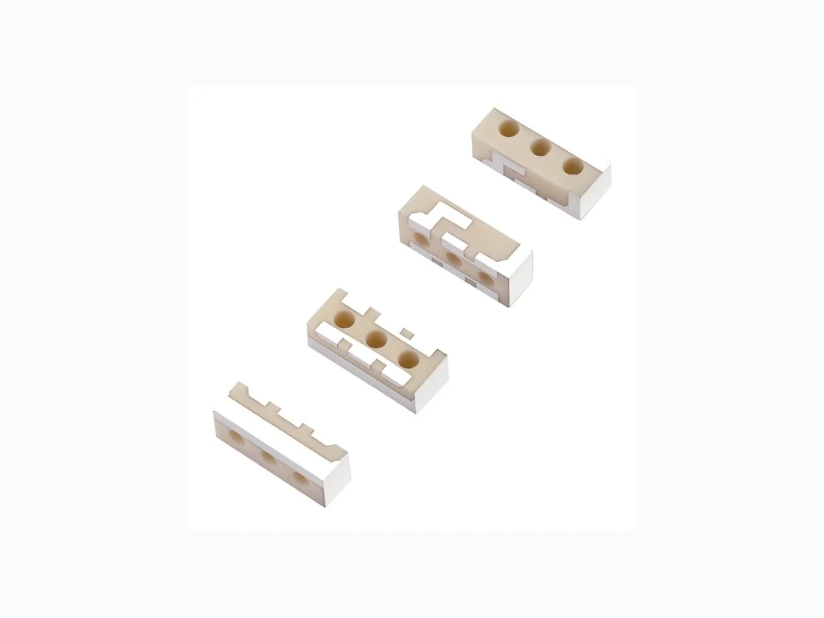
PA11 ETC2
Document overview
- Manufacturer or author: Provided By www.digicamel.com(FREE DATASHEET DOWNLOAD SITE)
- PDF pages: 18
Technical content
SPE-11-8-091/A 05-Sep-11 Page 1 of 1 SPECIFICATION Part No. : PA.11 Specification No : PA-2400-15-10-A-02 Product Name : 2.4GHz Band Dielectric Ceramic PIFA SMT Antenna for Bluetooth/WLAN/Zigbee
Applications
Description : 2400-2484Mhz, 1.5dBi Peak Gain Size: 10mm*4mm*3mm Designed for the top right hand corner edge of the Component side of the board (bottom left corner edge) SMT Mount RoHS Compliant
SPE-11-8-091/A 05-Sep-11 Page 2 of 2
1.0 Scope
This specification covers the Dielectric PIFA Antenna for 2400 -2484MHz, covering such applications as Wi-Fi, Bluetooth and Zigbee. A ceramic dielectric PIFA antenna offers smallest footprint, superior gain characteristics and improved isolation over traditional PCB based antennas. This antenna has been developed for the top righ t hand corner edge of the component side of the Board (bottom left corner edge), the antenna has to be positioned on a non -ground (copper/metal free) area with the feed-point matched direct to the module . Please refer to Recommended Foot print Diagram (8.0 Page 13.).
2.0 Electrical Specifications
The antenna has the electrical characteristics given in Table 1 under the Taoglas standard installation conditions as shown in the Evaluation Board. figure. No. Parameter Specification
1 Working Frequency 2400MHz ~ 2484MHz
2 Dimensions 10*4*3mm
3 Peak Gain 1.5 dBi max
4 Polarization Linear
5 Impedance 50 Ω
6 VSWR 2.0 max
7 Operating Temperature -40~+85°C
8 Termination Ag(Environmentally Friendly Lead-Free)
- Data is measured on Taoglas Standard Reference PCB
SPE-11-8-091/A 05-Sep-11 Page 3 of 3
3.0 S11 Response Curve
- Gain is measured on test PCB (40*80*0.8) * Ant position: Right side, top corner edge, horizontal
4.0 Test Position
x z y
SPE-11-8-091/A 05-Sep-11 Page 4 of 4
5.0 Summary of Test Results
5.1 Gain & Efficiency
Frequency (GHz) Peak Gain(dBi) Efficiency (%) 1 2.400 2.78 80.64 2 2.442 31.2 85.65 3 2.450 3.27 86.50 4 2.4835 2.76 75.91 5 2.500 2.34 68.07
5.2 Power Average Gain
Frequency (GHz) Plane Average Gain (dBi) 1 2.400 XY plane YZ plane XZ plane -1.622 -1.324 -0.561 2 2.442 XY plane YZ plane XZ plane -2.464 -0.859 -0.312 3 2.450 XY plane YZ plane XZ plane -1.424 -0.950 -0.224 4 2.4835 XY plane YZ plane XZ plane -2.949 -1.548 -0.784 5 2.500 XY plane YZ plane XZ plane -2.444 -2.084 -1.258
SPE-11-8-091/A 05-Sep-11 Page 5 of 5
6.0 Antenna Pattern – Wi-Fi & Bluetooth
Frequency: 2.400 GHz
SPE-11-8-091/A 05-Sep-11 Page 6 of 6 Frequency: 2.442 GHz
SPE-11-8-091/A 05-Sep-11 Page 7 of 7
SPE-11-8-091/A 05-Sep-11 Page 8 of 8 Frequency: 2.450 GHz
SPE-11-8-091/A 05-Sep-11 Page 9 of 9 Frequency: 2.4835 GHz
SPE-11-8-091/A 05-Sep-11 Page 10 of 10
SPE-11-8-091/A 05-Sep-11 Page 11 of 11 Frequency: 2.500 GHz
SPE-11-8-091/A 05-Sep-11 Page 12 of 12
7.0 Drawing
SPE-11-8-091/A 05-Sep-11 Page 13 of 13 Solder Area Silver Copper Ground Clearance Area
SPE-11-8-091/A 05-Sep-11 Page 14 of 14
8.0 Recommended foot print for Evaluation Board
SPE-11-8-091/A 05-Sep-11 Page 15 of 15
9.0 Delivery Mode
1 Blister tape to IEC 286-3,polyester
2 Pieces/tape:1000
Product code Units per Reel C (mm) D (mm) W2 (mm) PA.11 1000 330±1 62±0.5 24±1
SPE-11-8-091/A 05-Sep-11 Page 16 of 16 No Index Spec. (mm) 1 A 4.6 2 B 10.6
3 P1 12
4 W 24
5 F 8.5 6 T 3.5 7 D 1.5
SPE-11-8-091/A 05-Sep-11 Page 17 of 17
10.0 Recommended Reflow Temperature Profile
- Time shown in the above figures is measured from the point when chip surface reaches temperature. 2. Temperature difference in high temperature part should be within 110°C. 3. After soldering, do not force cool, allow the parts to cool gradually. *General attention to soldering:
- High soldering temperatures and long soldering times can cause leaching of the termination, decrease in adherence strength, and the change of characteristic may occur.
- For soldering, please refer to the soldering curves above. However, please keep exposure to temperatures exceeding 200°C to under 50 seconds.
- Please use a mild flux (containing less than 0.2wt% Cl). Also, if the flux is water soluble, be sure to wash thoroughly to remove any residue from the underside of components that could affect resistance.
SPE-11-8-091/A 05-Sep-11 Page 18 of 18 Cleaning: When using ultrasonic cleaning, the board may resonate if the output power is too high. Since this vibration can cause cracking or a decrease in the adherence of the termination, we recommend that you use the conditions below. Frequency: 40kHz Output Power: 20W/liter Cleaning Time: 5 minutes max