
DATASHEET SEARCH SITE
Document overview
- Manufacturer or author: Provided By digicamel.com
- PDF pages: 6
Technical content
Features
- Low-profile package
- Ideal for automated placement
- A v a i l a b l e i n U n i - d i r e c t i o n a l and Bi-directional
- 600 W peak pulse power capability with a 10/1000 μs waveform
- Excellent clamping capability
- Low incremental surge resistance
- V e r y f a s t r e s ponse time
- Meets MSL level 1, per J-STD-020, LF maximum peak of 260 °C
- Part no. with suffix “Q” means AEC-Q101 qualified Bi-directional Typical Applications For use in sensitive electronics protection against voltage transients induced by inductive load switching and lighting on ICs, MOSFET, signal lines of sensor units for consumer, automotive, and telecommunication. Mechanical Data
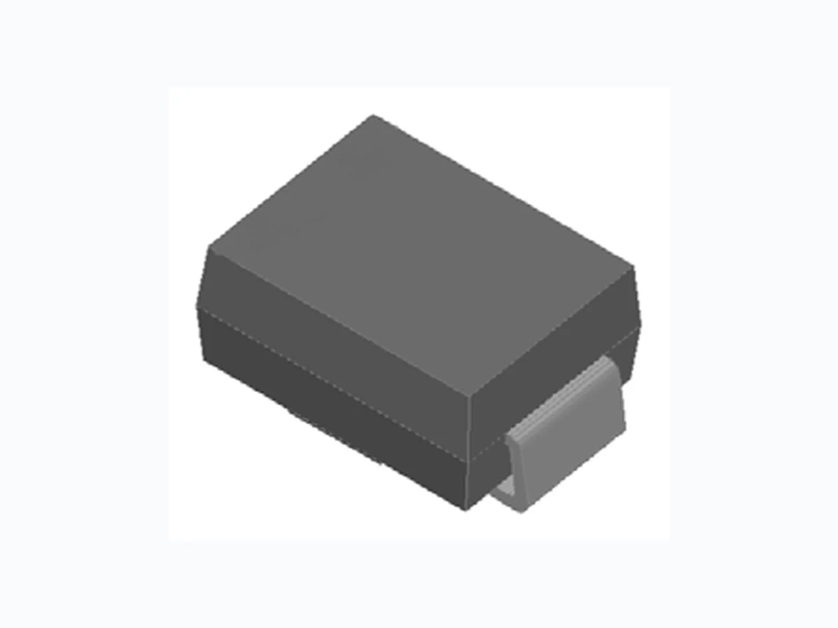
- Package: DO-214AA (SMB) Molding compound meets UL 94 V-0 flammability rating, RoHS-compliant, halogen-free
- Terminals: Matte tin plated leads, solderable per J-STD-002B and JESD22-B102D
- Polarity: For uni-directional types the band denotes cathode end, no marking on bi-directional types ■Maximum Ratings (Ta=25℃ Unless otherwise specified) PARAMETER SYMBOL UNIT Max Peak power dissipation, with a 10/1000us waveform (1) (2) (Fig.1) PPPM W 600 Peak pulse current, with a 10/1000us waveform(1) IPPM A See Next Table Peak forward surge current, 8.3 ms single half sine-wave unidirectional only (2) IFSM A 100 Operating junction and storage temperature range TJ,TSTG ℃ -55 to +150 ■Electrical Characteristics(Ta=25℃ Unless otherwise specified) PARAMETER SYMBOL UNIT VALUE Maximum instantaneous forward voltage @ at 50A for unidirectional only (3) VF V 3.5 COMPLIANT RoHS
Yangzhou Yangjie Electronic Technology Co., Ltd. S-S2689 Rev.1.0,21-Nov-19 www.21yangjie.com ■Thermal Characteristics (Ta=25℃ Unless otherwise specified) PARAMETER SYMBOL UNIT Conditions VALUE Thermal resistance(Typical) RθJL ℃/W junction to lead 20 RθJA ℃/W junction to ambient 100 Notes: (1) Non-repetitive current pulse, per Fig. 3 and derated above TA= 25 per Fig℃ .2. (3) V F<3.5V for devices of VBR<190V ■Ordering Information (Example) PREFERED P/N PACKING CODE UNIT WEIGHT(g) MINIMUM PACKAGE(pcs) INNER BOX QUANTITY(pcs) OUTER CARTON QUANTITY(pcs) DELIVERY MODE P6SMB12AQ- P6SMB220CAQ F1 0.1003 3000 6000 48000 13” reel ■Electrical Characteristics(Ta=25℃ Unless otherwise specified) Part Number (Uni) Part Number (Bi) Breakdown Voltage VBR@IT Maximum Reverse Leakage IR (6)@ VRWM (μA) Working Peak Reverse Voltage VRWM (V) Maximum Reverse Surge Current IPP (5) (A) Maximum Clamping Voltage Vc @ IPP (V) Min(V) Max (V) IT (4)(mA)
Yangzhou Yangjie Electronic Technology Co., Ltd. S-S2689 Rev.1.0,21-Nov-19 www.21yangjie.com ■Electrical Characteristics(Ta=25℃ Unless otherwise specified) Part Number (Uni) Part Number (Bi) Breakdown Voltage VBR@IT Maximum Reverse Leakage IR (6)@ VRWM (μA) Working Peak Reverse Voltage VRWM (V) Maximum Reverse Surge Current IPP (5) (A) Maximum Clamping Voltage Vc @ IPP (V) Min(V) Max (V) IT (4)(mA) Notes: (4) Pulse test: tp≤50ms. (5) Surge current waveform per Fig. 3 and derated per Fig.2.
Yangzhou Yangjie Electronic Technology Co., Ltd. S-S2689 Rev.1.0,21-Nov-19 www.21yangjie.com ■ Characteristics (Typical) 0.1μs 1μs 10μs 100μs 1.0ms 10ms 0.1 td(μs) PPPM(KW) FIG1:Peak Pulse Power Rating Curve 1.0 100 Non-Repetitive Pulse Waveform shown in Fige.3 Ta=25℃ Copper Pad Areas 0 200 TJ(℃) PPP or IPP(%) FIG2: Pulse Power or Current vs. Initial Junction Temperature 100 175150125100755025 04 . 0 t(ms) IPPM(%) FIG3: Pulse Waveform 150 100 3.02.01.0 TJ=25℃ Pulse Width(td) is defined as the Point where the Peak Current Decays to 50% of IPPM 10/1000μs Waveform as Defined by R.E.A. tr=10μs Peak Value IPPM Half Value - IPP IPPM td 0.001 0.01 0.1 1 10 1000 0.1 tp(s) Rth(/ W )℃ FIG4:Typical Transient Thermal Impedance 100 100 0 10 100 Number of Cycles Peak Forward Surge Current(A) FIG5: Maximum Non-Repetitive Surge Current 200 100 TJ=TJMax. 8.3ms Single Half Sine-Wave
Yangzhou Yangjie Electronic Technology Co., Ltd. S-S2689 Rev.1.0,21-Nov-19 www.21yangjie.com ■ Outline Dimensions ■ Suggested pad layout DO-214AA(SMB) Dim Millimeters P1 6.8 P2 4.3 P3 1.8 Q1 2.5 Q2 2.3 DO-214AA(SMB) Dim Min Max A 1.85 2.15 B 3.30 3.94 C 4.25 4.75 D 1.99 2.61 E 5.21 5.59 F 0.90 1.41 G 0.10 0.20 H 0.15 0.31 Dimensions in millimeters DO-214AA(SMB) A B C D E F HG Dimensions in millimeters
Yangzhou Yangjie Electronic Technology Co., Ltd. S-S2689 Rev.1.0,21-Nov-19 www.21yangjie.com Disclaimer The information presented in this document is for reference onl y. Yangzhou Yangjie Electronic Technology Co., Ltd. reserves th e right to make changes without not ice for the specification of t he products displayed herein to improve reliability, function o r design or otherwise. The product listed herein is designed to be used with automotive electronics,are not designed for use in medical, lifesaving, lifesust aining,or military,Yangjie or anyone on its behalf, assumes no responsibility or liability for any damages resulting from such improp er use of sale. This publication supersedes & replaces all information previously supplied. For additional information, please visit our website http:// www.21yangjie.com , or consult your nearest Yangjie’s sales office for further assistance.