

 Download PDF
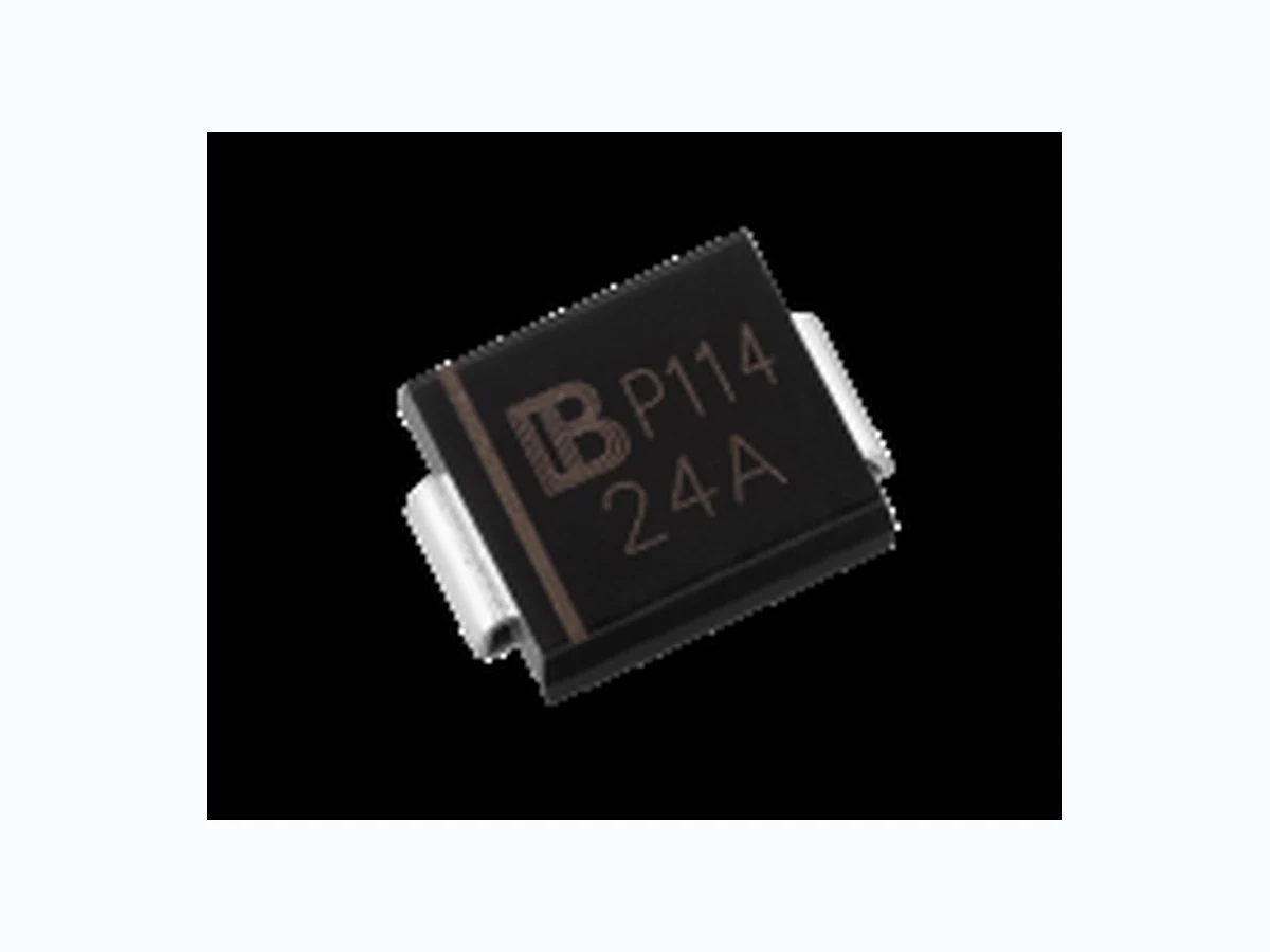
P4SMA-AT YAGEO
Document overview
- PDF pages: 9
Technical content
Page 1
DATA SHEET
TRANSIENT VOLTAGE SUPPRESSORS
AC/DC POWER SUPPLY P4SMA-AT series RoHS compliant & Halogen free
Page 2

Transient Voltage Suppressors (TVS) Data Sheet
Features
■ For surface mounted applications in order to optimize board space
■ Low profile package ■ Glass passivated junction ■ Low inductance ■ Excellent clamping capability ■ 400W peak pulse power capability at 10/1000μs waveform, repetition rate (duty cycle): 0.01% ■ Fast response time ■ Typical IR less than 1μA above 10V ■ High Temperature soldering: 260℃/10 seconds at terminals ■ Plastic package has underwriters laboratory flammability 94V-0 ■ Meets MSL level 1, per J-STD-020 ■ Safety certification: UL ■ AEC-Q101 qualified ■ IEC61000-4-2 ESD 30KV Air, 30KV contact compliance
Mechanical Data
■ Case: JEDEC DO-214AC. Molded plastic over glass passivated junction ■ Terminal: Tin plated, solderable per MIL-STD-750, Method 2026 ■ Polarity: Color band denotes cathode except bi-directional models ■ Standard Packaging: 12mm tape (EIA STD RS-481) ■ Weight: 0.07g
Applications
■ I/O interface ■ AC/DC power supply ■ Low frequency signal transmission line (RS232, RS485, etc.)
Maximum Ratings and Characteristics
Ratings at 25℃ ambient temperature unless otherwise specified.
| Rating | Symbol | Value | Units |
|---|---|---|---|
| Peak pulse power dissipation at 10/1000μs waveform (Note1, Note2, Fig.1) | P PPM | Minimum 400 | Watts |
| Peak pulse current of at 10/1000μs waveform (Note 1, Fig.3) | I PPM | See Table | Amps |
| Steady state power dissipation at T =50℃ (Fig.5) A | P M(AV) | 3.3 | Watts |
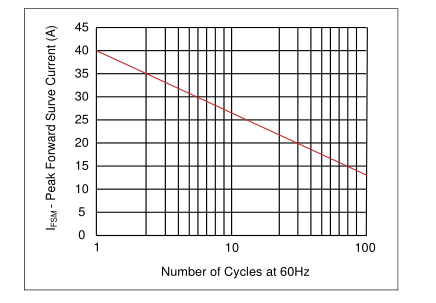
| Peak forward surge current, 8.3ms single half sine-wave superimposed on rated load, (JEDEC Method) (Note3, Fig.6) | I FSM | 40 | Amps |
| Operating junction and Storage Temperature Range. | T ,T J STG | -55 to +150 | ℃ |
| Typical thermal resistance junction to lead | RθJL | 30 | ℃/W |
| Typical thermal resistance junction to ambient | RθJA | 120 | ℃/W |
Notes: 1. Non-repetitive current pulse, per Fig.3 and derated above TA=25℃ per Fig.2. 2. Mounted on 5.0mm×5.0mm (0.03mm thick) copper pads to each terminal. 3. 8.3ms single half sine-wave, or equivalent square wave, duty cycle=4 pulses per minutes maximum.
Page 3

Dimensions (SMA/DO-214AC)
| Product: Cathode Band D1 D L H1 H d T1 T Pad: 1.68mm 1.75mm 1.88mm 1.75mm | Symbol | Millimeters | Inches | ||
| Min. | Max. | Min. | Max. | ||
| L | 3.99 | 4.50 | 0.157 | 0.177 | |
| D | 2.54 | 2.79 | 0.100 | 0.110 | |
| D1 | 1.25 | 1.65 | 0.049 | 0.065 | |
| T | 4.93 | 5.28 | 0.194 | 0.208 | |
| T1 | 0.76 | 1.52 | 0.030 | 0.060 | |
| d | - | 0.203 | - | 0.008 | |
| H | 2.00 | 2.50 | 0.079 | 0.098 | |
| H1 | 1.98 | 2.29 | 0.078 | 0.090 | |
Electrical Characteristics (TA=25℃)
| Part Number | Device Marking Code | Reverse Stand-Off Voltage | Breakdown Voltage @IT | Test Current | Maximum Clamping Voltage @IPP | Peak Pulse Current | Reverse Leakage @VRWM | ||
|---|---|---|---|---|---|---|---|---|---|
| Unidirectional | Bidirectional | UNI | BI | VRWM(V) | VBR(V) | IT(mA) | VC(V) | IPP(A) | IR(μA) |
| P4SMA6.8A-AT | P4SMA6.8CA-AT | 6V8A | 6V8C | 5.80 | 6.45~7.14 | 10 | 10.5 | 39.0 | 1000 |
| P4SMA7.5A-AT | P4SMA7.5CA-AT | 7V5A | 7V5C | 6.40 | 7.13~7.88 | 10 | 11.3 | 36.3 | 500 |
| P4SMA8.2A-AT | P4SMA8.2CA-AT | 8V2A | 8V2C | 7.02 | 7.79~8.61 | 10 | 12.1 | 33.9 | 200 |
| P4SMA9.1A-AT | P4SMA9.1CA-AT | 9V1A | 9V1C | 7.78 | 8.65~9.55 | 1 | 13.4 | 30.6 | 50 |
| P4SMA10A-AT | P4SMA10CA-AT | 10A | 10C | 8.55 | 9.50~10.50 | 1 | 14.5 | 28.3 | 10 |
| P4SMA11A-AT | P4SMA11CA-AT | 11A | 11C | 9.40 | 10.50~11.60 | 1 | 15.6 | 26.3 | 5 |
| P4SMA12A-AT | P4SMA12CA-AT | 12A | 12C | 10.20 | 11.40~12.60 | 1 | 16.7 | 24.6 | 5 |
| P4SMA13A-AT | P4SMA13CA-AT | 13A | 13C | 11.10 | 12.40~13.70 | 1 | 18.2 | 22.5 | 1 |
| P4SMA15A-AT | P4SMA15CA-AT | 15A | 15C | 12.80 | 14.30~15.80 | 1 | 21.2 | 19.3 | 1 |
| P4SMA16A-AT | P4SMA16CA-AT | 16A | 16C | 13.60 | 15.20~16.80 | 1 | 22.5 | 18.2 | 1 |
| P4SMA18A-AT | P4SMA18CA-AT | 18A | 18C | 15.30 | 17.10~18.90 | 1 | 25.2 | 16.1 | 1 |
| P4SMA20A-AT | P4SMA20CA-AT | 20A | 20C | 17.10 | 19.00~21.00 | 1 | 27.7 | 14.8 | 1 |
| P4SMA22A-AT | P4SMA22CA-AT | 22A | 22C | 18.80 | 20.90~23.10 | 1 | 30.6 | 13.4 | 1 |
| P4SMA24A-AT | P4SMA24CA-AT | 24A | 24C | 20.50 | 22.80~25.20 | 1 | 33.2 | 12.3 | 1 |
Page 4

| Part Number | Device Marking Code | Reverse Stand-Off Voltage | Breakdown Voltage @IT | Test Current | Maximum Clamping Voltage @IPP | Peak Pulse Current | Reverse Leakage @VRWM | ||
|---|---|---|---|---|---|---|---|---|---|
| Unidirectional | Bidirectional | UNI | BI | VRWM(V) | VBR(V) | IT(mA) | VC(V) | IPP(A) | IR(μA) |
| P4SMA27A-AT | P4SMA27CA-AT | 27A | 27C | 23.10 | 25.70~28.40 | 1 | 37.5 | 10.9 | 1 |
| P4SMA30A -AT | P4SMA30CA-AT | 30A | 30C | 25.60 | 28.50~31.50 | 1 | 41.4 | 9.9 | 1 |
| P4SMA33A-AT | P4SMA33CA-AT | 33A | 33C | 28.20 | 31.40~34.70 | 1 | 45.7 | 9.0 | 1 |
| P4SMA36A-AT | P4SMA36CA-AT | 36A | 36C | 30.80 | 34.20~37.80 | 1 | 49.9 | 8.2 | 1 |
| P4SMA39A-AT | P4SMA39CA-AT | 39A | 39C | 33.30 | 37.10~41.00 | 1 | 53.9 | 7.6 | 1 |
| P4SMA43A-AT | P4SMA43CA-AT | 43A | 43C | 36.80 | 40.90~45.20 | 1 | 59.3 | 6.9 | 1 |
| P4SMA47A-AT | P4SMA47CA-AT | 47A | 47C | 40.20 | 44.70~49.40 | 1 | 64.8 | 6.3 | 1 |
| P4SMA51A-AT | P4SMA51CA-AT | 51A | 51C | 43.60 | 48.50~53.60 | 1 | 70.1 | 5.8 | 1 |
| P4SMA56A-AT | P4SMA56CA-AT | 56A | 56C | 47.80 | 53.20~58.80 | 1 | 77.0 | 5.3 | 1 |
| P4SMA62A-AT | P4SMA62CA-AT | 62A | 62C | 53.00 | 58.90~65.10 | 1 | 85.0 | 4.8 | 1 |
| P4SMA68A-AT | P4SMA68CA-AT | 68A | 68C | 58.10 | 64.60~71.40 | 1 | 92.0 | 4.5 | 1 |
| P4SMA75A-AT | P4SMA75CA-AT | 75A | 75C | 64.10 | 71.30~78.80 | 1 | 103.0 | 4.0 | 1 |
| P4SMA82A-AT | P4SMA82CA-AT | 82A | 82C | 70.10 | 77.90~86.10 | 1 | 113.0 | 3.6 | 1 |
| P4SMA91A-AT | P4SMA91CA-AT | 91A | 91C | 77.80 | 86.50~95.50 | 1 | 125.0 | 3.3 | 1 |
| P4SMA100A-AT | P4SMA100CA-AT | 100A | 100C | 85.50 | 95.00~105.00 | 1 | 137.0 | 3.0 | 1 |
| P4SMA110A-AT | P4SMA110CA-AT | 110A | 110C | 94.00 | 105.00~116.00 | 1 | 152.0 | 2.7 | 1 |
| P4SMA120A-AT | P4SMA120CA-AT | 120A | 120C | 102.00 | 114.00~126.00 | 1 | 165.0 | 2.5 | 1 |
| P4SMA130A-AT | P4SMA130CA-AT | 130A | 130C | 111.00 | 124.00~137.00 | 1 | 179.0 | 2.3 | 1 |
| P4SMA150A-AT | P4SMA150CA-AT | 150A | 150C | 128.00 | 143.00~158.00 | 1 | 207.0 | 2.0 | 1 |
| P4SMA160A-AT | P4SMA160CA-AT | 160A | 160C | 136.00 | 152.00~168.00 | 1 | 219.0 | 1.9 | 1 |
| P4SMA170A-AT | P4SMA170CA-AT | 170A | 170C | 145.00 | 162.00~179.00 | 1 | 234.0 | 1.8 | 1 |
| P4SMA180A-AT | P4SMA180CA-AT | 180A | 180C | 154.00 | 171.00~189.00 | 1 | 246.0 | 1.7 | 1 |
| P4SMA200A-AT | P4SMA200CA-AT | 200A | 200C | 171.00 | 190.00~210.00 | 1 | 274.0 | 1.5 | 1 |
| P4SMA220A-AT | P4SMA220CA-AT | 220A | 220C | 185.00 | 209.00~231.00 | 1 | 328.0 | 1.3 | 1 |
| P4SMA250A-AT | P4SMA250CA-AT | 250A | 250C | 214.00 | 237.00~263.00 | 1 | 344.0 | 1.2 | 1 |
| P4SMA300A-AT | P4SMA300CA-AT | 300A | 300C | 256.00 | 285.00~315.00 | 1 | 414.0 | 1.0 | 1 |
| P4SMA350A-AT | P4SMA350CA-AT | 350A | 350C | 300.00 | 332.00~368.00 | 1 | 482.0 | 0.9 | 1 |
| P4SMA400A-AT | P4SMA400CA-AT | 400A | 400C | 342.00 | 380.00~420.00 | 1 | 548.0 | 0.8 | 1 |
| P4SMA440A-AT | P4SMA440CA-AT | 440A | 440C | 376.00 | 418.00~462.00 | 1 | 602.0 | 0.7 | 1 |
| P4SMA480A-AT | P4SMA480CA-AT | 480A | 480C | 408.00 | 456.00~504.00 | 1 | 658.0 | 0.6 | 1 |
| P4SMA510A-AT | P4SMA510CA-AT | 510A | 510C | 434.00 | 485.00~535.00 | 1 | 698.0 | 0.6 | 1 |
| P4SMA530A-AT | P4SMA530CA-AT | 530A | 530C | 450.00 | 503.50~556.50 | 1 | 725.0 | 0.6 | 1 |
| P4SMA540A-AT | P4SMA540CA-AT | 540A | 540C | 459.00 | 513.00~567.00 | 1 | 740.0 | 0.5 | 1 |
| P4SMA550A-AT | P4SMA550CA-AT | 550A | 550C | 467.00 | 522.50~577.50 | 1 | 760.0 | 0.5 | 1 |
| P4SMA600A-AT | P4SMA600CA-AT | 600A | 600C | 510.00 | 570.00~630.00 | 1 | 828.0 | 0.48 | 1 |
Page 5

Ratings and Characteristic Curves (TA=25℃ unless otherwise noted)
Figure 1. Peak Pulse Power Rating Curve
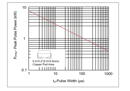
Figure 3. Pulse Waveform
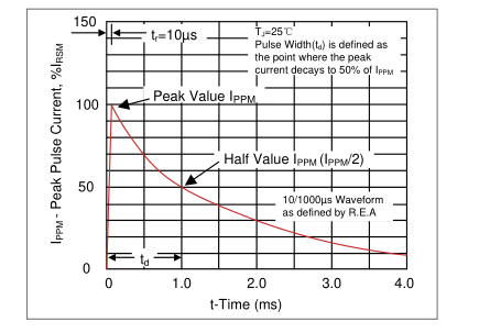
Figure 5. Steady State Power Dissipation Derating
Curve
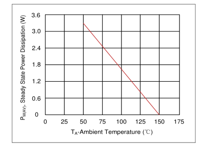
Figure 2. Pulse Derating Curve
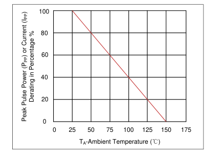
Figure 4. Typical Junction Capacitance
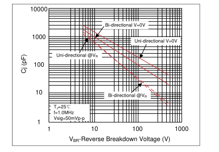
Figure 6. Maximum Non-Repetitive Forward Surge Current Uni-Directional Only
Page 6

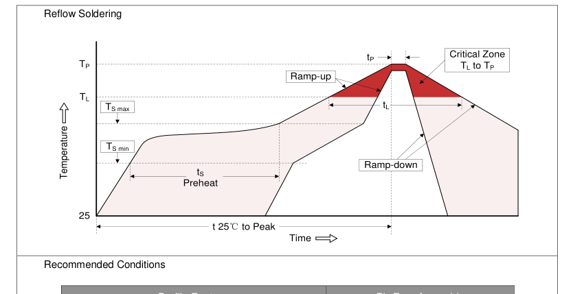
Recommended Soldering Conditions
| Profile Feature | Pb-Free Assembly |
| Average ramp-up rate (T to T ) L P | 3℃/second max. |
| Preheat -Temperature Min (T ) S min -Temperature Max (T ) S max -Time (min to max) (t ) S | 150℃ 200℃ 60-180 seconds |
| T to T S max L -Ramp-up Rate | 3℃/second max. |
| Time maintained above: -Temperature (T ) L -Time (t ) L | 217℃ 60-150 seconds |
| Peak Temperature (T ) P | 260℃ |
| Time within 5℃ of actual Peak Temperature (t ) P | 20-40 seconds |
| Ramp-down Rate | 6℃/second max. |
| Time 25℃ to Peak Temperature | 8 minutes max. |
Page 7

Marking Code
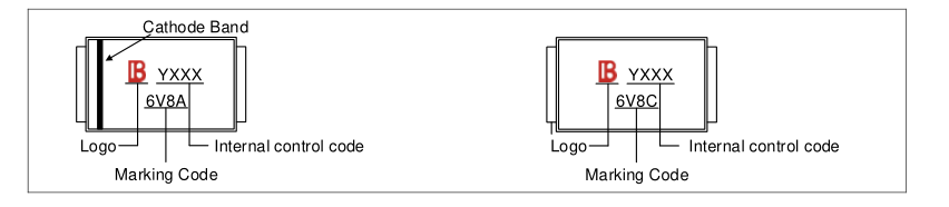
Part Number Code
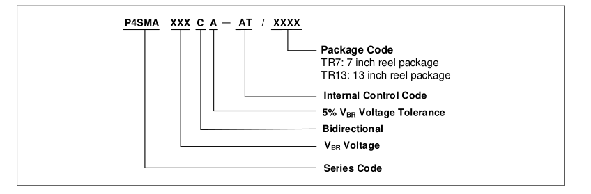
Ordering Code for Different Package
7 inch reel package: Add suffix “ /TR7 ” at the end of the part number, such as P4SMAXXXCA-AT/TR7 13 inch reel package: Add suffix “ /TR13 ” at the end of the part number, such as P4SMAXXXCA-AT/TR13
Page 8

Packaging
| Tape P0 P1 P2 D0 B E T F W B0 D1 A A B K0 SECTION B-B A0 SECTION A-A | Symbol | Dimension (mm) |
| W | 12.00±0.20 | |
| P0 | 4.00±0.10 | |
| P1 | 4.00±0.10 | |
| P2 | 2.00±0.10 | |
| D0 | Φ1.5±0.10 | |
| D1 | Φ1.5±0.10 | |
| E | 1.75±0.10 | |
| F | 5.50±0.05 | |
| A0 | 2.79±0.10 | |
| B0 | 5.33±0.10 | |
| K0 | 2.55±0.15 | |
| T | 0.25±0.05 | |
| 7” Reel D4 D3 D2 W1 | D2 | Φ178.0±2.0 |
| D3 | Φ50.0Min. | |
| D4 | Φ13.0±0.5 | |
| W1 | 16.0±2.0 | |
| Quantity: 1000PCS | ||
| 13” Reel | D5 | Φ330.0±2.0 |
| D6 | Φ13.5±0.5 | |
| H | 2.5±1.0 | |
| W2 | 16.0±2.0 | |
| Quantity: 5000PCS | ||
Page 9
Product specification
Circuit Protection Components
LEGAL DISCLAIMER
YAGEO, its distributors and agents (collectively, “YAGEO”), hereby disclaims any and all liabilities for any errors, inaccuracies or incompleteness contained in any product related information, including but not limited to product specifications, datasheets, pictures and/or graphics. YAGEO may make changes, modifications and/or improvements to product related information at any time and without notice.
YAGEO makes no representation, warranty, and/or guarantee about the fitness of its products for any particular purpose or the continuing production of any of its products. To the maximum exten t permitted by law, YAGEO disclaims (i) any and all liability arising out of the application or use of any YAGEO product, (ii) any and all liability, including without limitation special, consequential or incidental damages, and (iii) any and all implied warranties, including warranties of fitness for a particular purpose, non -infringement and merchantability.
YAGEO products are designed for general purpose applications under normal operation and usage conditions. Please contact YAGEO for the applications listed below which require especially high reliability for the prevention of defects which might directly cause damage to the third party's life, body or property: Aerospace equipment (artificial satellite, rocket, etc.), Atomic energy-related equipment, Aviation equipment, Disaster prevention equipment, crime prevention equipment, Electric heating apparatus, burning equipment, Highly public information network equipment, data-processing equipment , Medical devices, Military equipment, Power generation control equipment, Safety equipment, Traffic signal equipment, Transportation equipment and
Undersea equipment, or for any other application or use in which the failure of YAGEO products could result in personal injury or death, or serious property damage. Particularly YAGEO Corporation and its affiliates do not recommend the use of commercial or automotive grade products for high reliability applications or manned space flight.
Information provided here is intended to indicate product specifications only. YAGEO reserves all the rights for revising this content without further notification, as long as products are unchanged. Any product change will be announced by PCN.