
P4KE6.8 VISHAY
Document overview
- Manufacturer or author: Provided By www.digicamel.com(free datasheet download site)
- PDF pages: 6
Technical content
P4KE6.8 thru P4KE540A Vishay General Semiconductor Document Number: 88365 Revision: 22-Oct-08 For technical questions within your region, please contact one of the following: PDD-Americas@vishay.com , PDD-Asia@vishay.com , PDD-Europe@vishay.com www.vishay.com TRANSZORB® Transient Voltage Suppressors
FEATURES
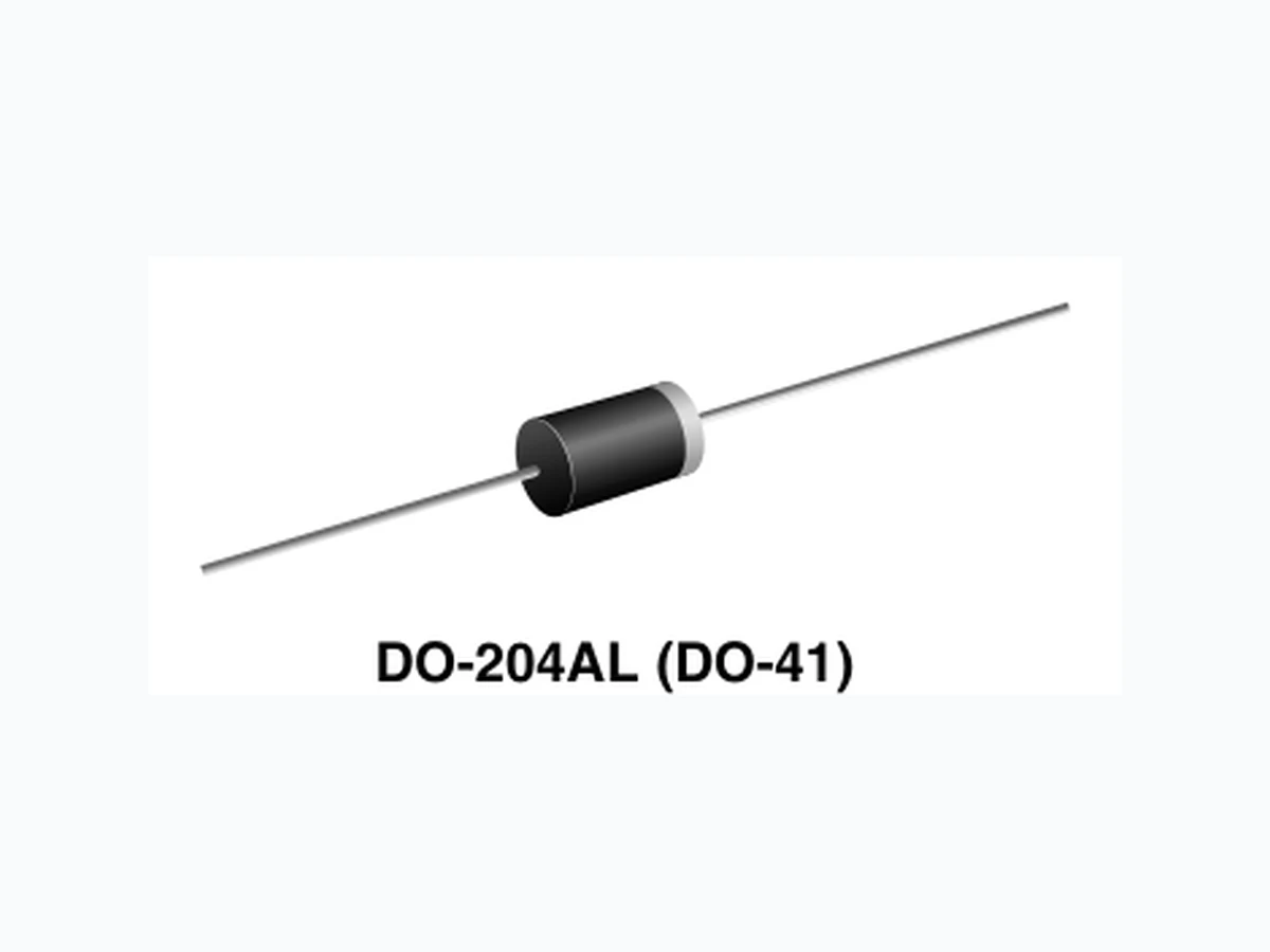
- Glass passivated chip junction Available in uni-directional and bi-directional 400 W peak pulse power capability with a 10/1000 µs waveform, repetitive rate (duty cycle): 0.01 % Excellent clamping capability Very fast response time Low incremental surge resistance Solder dip 260 °C, 40 s Component in accordance to RoHS 2002/95/EC and WEEE 2002/96/EC TYPICAL APPLICATIONS Use in sensitive electronics protection against voltage transients induced by inductive load switching and lighting on ICs, MOSFET, signal lines of sensor units for consumer, computer, industrial, automotive and telecommunication. MECHANICAL DATA Case: DO-204AL, molded epoxy over passivated chip Molding compound meets UL 94 V-0 flammability rating Base P/N-E3 - RoHS compliant, commercial grade Base P/NHE3 - RoHS co mpliant, high reliability/ automotive grade (AEC Q101 qualified) Terminals: Matte tin plated leads, solderable per J-STD-002 and JESD22-B102 E3 suffix meets JESD 201 class 1A whisker test, HE3 suffix meets JESD 201 class 2 whisker test Note: P4KE250 ~ P4KE540A and P4KE250C ~ P4KE440CA for commercial grade only Polarity: For uni-directional types the color band denotes cathode end, no marking on bi-directional types DEVICES FOR BI-DIRECTION APPLICATIONS For bi-direction use C or CA suffix (e.g. P4KE440CA). Electrical characteristics apply in both directions. PRIMARY CHARACTERISTICS VBR uni-directional 6.8 V to 540 V VBR bi-directional 6.8 V to 440 V PPPM 400 W PD 1.5 W IFSM (uni-directional only) 40 A TJ max. 175 °C DO-204AL (DO-41) Notes: (1) Non-repetitive current pulse, per Fig. 3 and derated above TA = 25 °C per Fig. 2 (2) Measured on 8.3 ms single half sine-wave or equivalent square wave, duty cycle = 4 pulses per minute maximum (3) VF = 3.5 V for P4KE220(A) and below; VF = 5.0 V for P4KE250(A) and above MAXIMUM RATINGS (TA = 25 °C unless otherwise noted) PARAMETER SYMBOL LIMIT UNIT Peak power dissipation with a 10/1000 µs waveform (1) (Fig. 1) P PPM 400 W Peak pulse current with a 10/1000 µs waveform (1) I PPM See next table A Power dissipation on infinite heatsink at TL = 75 °C (Fig. 5) P D 1.5 W Peak forward surge current, 8.3 ms single half sine-wave uni-directional only (2) I FSM 40 A Maximum instantaneous forward voltage at 25 A for uni-directional only (3) V F 3.5/5.0 V Operating junction and storage temperature range T J, TSTG - 55 to + 175 °C
P4KE6.8 thru P4KE540A Vishay General Semiconductor www.vishay.com For technical questions within your region, please contact one of the following: PDD-Americas@vishay.com , PDD-Asia@vishay.com , PDD-Europe@vishay.com Document Number: 88365 Revision: 22-Oct-082 ELECTRICAL CHARACTERISTICS (TA = 25 °C unless otherwise noted) DEVICE TYPE BREAKDOWN VOLTAGE VBR AT IT (1) (V) TEST CURRENT IT (mA) STAND- OFF VOLTAGE VWM (V) MAXIMUM REVERSE LEAKAGE AT VWM ID (3) (µA) MAXIMUM PEAK PULSE CURRENT IPPM (2) (A) MAXIMUM CLAMPING VOLTAGE AT IPPM VC (V) MAXIMUM TEMPERATURE COEFFICIENT OF VBR (%/°C) MIN. MAX.
P4KE6.8 thru P4KE540A Vishay General Semiconductor Document Number: 88365 Revision: 22-Oct-08 For technical questions within your region, please contact one of the following: PDD-Americas@vishay.com , PDD-Asia@vishay.com , PDD-Europe@vishay.com www.vishay.com Notes: (1) Pulse test: tp ≤ 50 ms (2) Surge current waveform per Fig. 3 and derated per Fig. 2 (3) For bi-directional types having VWM of 10 V and less, the ID limit is doubled (4) All terms and symbols are consistent with ANSI/IEEE C62.35 P4KE120A 114 126 1.0 102 1.0 2.4 165 0.107 P4KE130 117 143 1.0 105 1.0 2.1 187 0.107 P4KE130A 124 137 1.0 111 1.0 2.2 179 0.107 P4KE150 135 165 1.0 121 1.0 1.9 215 0.108 P4KE150A 143 158 1.0 128 1.0 1.9 207 0.108 P4KE160 144 176 1.0 130 1.0 1.7 230 0.108 P4KE160A 152 168 1.0 136 1.0 1.8 219 0.108 P4KE170 153 187 1.0 138 1.0 1.6 244 0.108 P4KE170A 162 179 1.0 145 1.0 1.7 234 0.108 P4KE180 162 198 1.0 146 1.0 1.6 258 0.108 P4KE180A 171 189 1.0 154 1.0 1.6 246 0.108 P4KE200 180 220 1.0 162 1.0 1.4 287 0.108 P4KE200A 190 210 1.0 171 1.0 1.5 274 0.108 P4KE220 198 242 1.0 175 1.0 1.2 344 0.108 P4KE220A 209 231 1.0 185 1.0 1.2 328 0.108 P4KE250 225 275 1.0 202 1.0 1.1 360 0.110 P4KE250A 237 263 1.0 214 1.0 1.2 344 0.110 P4KE300 270 330 1.0 243 1.0 0.93 430 0.110 P4KE300A 285 315 1.0 256 1.0 1.0 414 0.110 P4KE350 315 385 1.0 284 1.0 0.79 504 0.110 P4KE350A 333 368 1.0 300 1.0 0.83 482 0.110 P4KE400 360 440 1.0 324 1.0 0.70 574 0.110 P4KE400A 380 420 1.0 342 1.0 0.73 548 0.110 P4KE440 396 484 1.0 356 1.0 0.63 631 0.110 P4KE440A 418 462 1.0 376 1.0 0.66 602 0.110 P4KE480 432 528 1.0 389 1.0 0.58 686 0.110 P4KE480A 456 504 1.0 408 1.0 0.61 658 0.110 P4KE510 459 561 1.0 413 1.0 0.55 729 0.110 P4KE510A 485 535 1.0 434 1.0 0.57 698 0.110 P4KE540 486 594 1.0 437 1.0 0.52 772 0.110 P4KE540A 513 567 1.0 459 1.0 0.54 740 0.110 THERMAL CHARACTERISTICS (TA = 25 °C unless otherwise noted) PARAMETER SYMBOL LIMIT UNIT Typical thermal resistance, junction to lead R θJL 66 °C/W Typical thermal resistance, junction to ambient, LLead = 10 mm R θJA 100 °C/W ELECTRICAL CHARACTERISTICS (TA = 25 °C unless otherwise noted) DEVICE TYPE BREAKDOWN VOLTAGE VBR AT IT (1) (V) TEST CURRENT IT (mA) STAND- OFF VOLTAGE VWM (V) MAXIMUM REVERSE LEAKAGE AT VWM ID (3) (µA) MAXIMUM PEAK PULSE CURRENT IPPM (2) (A) MAXIMUM CLAMPING VOLTAGE AT IPPM VC (V) MAXIMUM TEMPERATURE COEFFICIENT OF VBR (%/°C) MIN. MAX.
Document Number: 91000 www.vishay.com Revision: 18-Jul-08 1 Disclaimer Legal Disclaimer Notice Vishay All product specifications and data are subject to change without notice. Vishay Intertechnology, Inc., its affiliates, agents, and employees, and all persons acting on its or their behalf (collectively, “Vishay”), disclaim any and all liability for any errors, inaccuracies or incompleteness contained herein or in any other disclosure relating to any product. Vishay disclaims any and all li ability arising out of the use or application of any product described herein or of any information provided herein to the maximum extent permit ted by law. The product specifications do not expand or otherwise modify Vishay’s terms and conditions of purcha se, including but not limited to the warranty expressed therein, which apply to these products. No license, express or implied, by estoppel or otherwise, to any intellectual property rights is granted by this document or by any conduct of Vishay. The products shown herein are not designed for use in medi cal, life-saving, or life-sustaining applications unless otherwise expressly indicated. Customers using or selling Vishay products not expressly indicated for use in such applications do so entirely at their own risk and agree to fully indemnify Vishay for any damages arising or resulting from such use or sale. Please contact authorized Vishay personnel to obtain written terms and conditions regarding products designed for such applications. Product names and markings noted herein may be trademarks of their respective owners.