
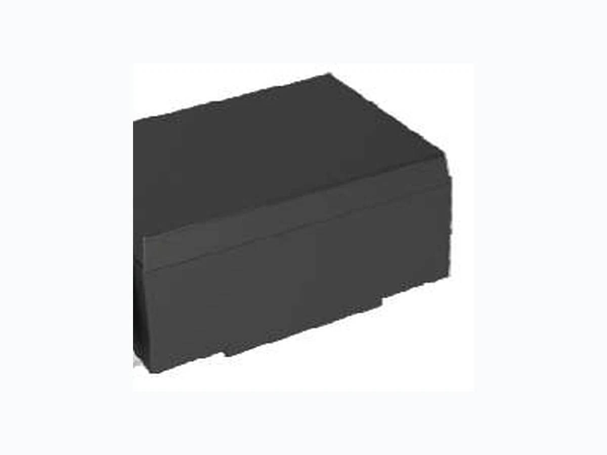
PXXXXTA LEIDITECH
Document overview
- Manufacturer or author: Provided By www.digicamel.com(FREE DATASHEET DOWNLOAD SITE)
- PDF pages: 5
Technical content
DESCRIPTION: PxxxxTA series thyristors are a type of semi component. They are designed equipment from damaging overvoltage transients. such as modems, telephones, line cards, answering machines, FAX machines, T1/E1, xDSL and more. FEATURES: Excellent c apability of absorbing transient surge Quick response to surge voltage (ns Level) Eliminates overvoltage caused by fast rising transients Moisture sensitivity level: Level 1 Fails short circuit when surged in excess of ratings Non degenerative ABSOLUTE MAXIMUM RATINGS Parameter Storage temperature range Operating junction temperature range Repetitive peak pulse current
ELECTRICAL CHARACTERISTICS
V DRM Peak off- state voltage I DRM Off- state current V S Switching voltage I S Switching current V T On- state voltage I T On- state current I H Holding current C O Off-state capacitance thyristors are a type of semi -conduct component. They are designed to protect baseband equipment from damaging overvoltage transients. modems, telephones, line cards, answering machines, FAX machines, T1/E1, xDSL and more. apability of absorbing transient surge Quick response to surge voltage (ns Level) Eliminates overvoltage caused by fast rising transients Moisture sensitivity level: Level 1 Fails short circuit when surged in excess of ratings RATINGS A =25ºC, RH=45%-75%, unless otherwise Parameter Symbol Value Storage temperature range T stg 60 to +150 junction temperature range T j 40 to +1 Repetitive peak pulse current I PP A =25℃) Parameter state voltage state current Switching voltage Switching current state voltage state current capacitance V-I Curve I T I DRM V I S I H unless otherwise noted) Value Unit 60 to +150 40 to +1 25 ℃ A SMA Symbol V T V DRM V S Rev : www.leiditech.com 01.06.2015 1/5
A =25℃,continued) Part Number I DRM DRM V S S V T @ I T I H C O μA V V mA V A mA pF max min max max max max min max P0080TA 5 6 25 800 4 2.2 20 30 P0220TA 5 15 32 800 4 2.2 20 60 P0300TA 5 25 40 800 4 2.2 50 60 P0640TA 5 58 77 800 4 2.2 120 50 P0720TA 5 65 87 800 4 2.2 120 50 P0900TA 5 75 98 800 4 2.2 120 50 P1100TA 5 90 130 800 4 2.2 120 45 P1300TA 5 120 160 800 4 2.2 120 45 P1500TA 5 140 180 800 4 2.2 120 45 P1800TA 5 170 220 800 4 2.2 120 35 P2300TA 5 190 260 800 4 2.2 120 35 P2600TA 5 220 300 800 4 2.2 120 35 P3100TA 5 275 350 800 4 2.2 120 35 P3500TA 5 320 400 800 4 2.2 120 35 P3800TA 5 340 450 800 4 2.2 120 35 Vs is measured at 100KV/① s ② Off-state capacitance is measured in V DC =2V, V RMS =1V, f=1MHz Surge Ratings Series I PP (A)min 2×10us 8×20us 10×360us 10×1000us A 150 150 70 50 Rev : www.leiditech.com 01.06.2015 2/5 PxxxxTA Series
ORDERING INFORMATION
P:SIDACtor Median Voltage Package type Surge Ratings :3KV(10/700us) 0:Bi-direction,1:Uni SOLDERING PARAMETERS Reflow Condition Pb-Free assembly (see FIG.2) Pre Heat -Temperature Min (T s(min) ) +150℃ -Temperature Max(T s(max) ) +200℃ -Time (Min to Max) (ts) 60-180 secs. Average ramp up rate (Liquid us Temp (T L ) to peak) 3℃/sec. Max T s(max) to T L - Ramp-up Rate 3℃/sec. Max Reflow -Temperature(T L ) (Liquid us) +217℃ -Temperature(t L ) 60-150 secs. Peak Temp (T p ) +260(+0/-5)℃ Time within 5℃ of actual Peak Temp (t p ) 30 secs. Max Ramp-down Rate 6℃/sec. Max Time 25℃ to Peak Temp (T P ) 8 min. Max Do not exceed +260℃ Rev : www.leiditech.com 01.06.2015 3/5 PxxxxTA Series
FIG.1: tr × td pulse waveform PP 100 t r t d t(μs) Peak value tr = rise time to peak value td = decay time to half value Half value FIG.2: Reflow condition Temperature T S(min) T S(max) T L T P tp t L time to peak temperatue Time (t 25 to peak)℃ Ramp-up Ramp-down Preheat Critical Zone T L to T P t s FIG.3: Normalized Vs change vs. junction temperature FIG.4: Normalized DC holding current vs. case temperature I H j )/I H j =25 ) 0.4-40 -20 100 120 140 160 T j ( ) Percent of Vs change(%) 2.0 1.24 T C ( ) -40 -20 100 120 140 160 0.8 1.6 0.6 1.0 1.4 1.8 PACKAGE MECHANICAL DATA Dimensions Millimeters InchesRef. Min. A B C D E F G 4.25 2.50 1.35 0.76 4.93 0.15 0.051 A B DO-214AC (SMA) D E F G H H 1.98 Max. 4.65 2.90 1.65 1.52 5.28 0.203 0.31 2.41 Min. 0.167 0.098 0.053 0.030 0.194 0.002 0.006 0.078 Max. 0.183 0.114 0.065 0.060 0.208 0.008 0.012 0.095 K J J K 6.50 L 1.70 2.30 0.256 0.067 0.090 L Rev : www.leiditech.com 01.06.2015 4/5 PxxxxTA Series
TAPE AND REEL SPECIFICATION-SMA E F d P A B W OUTLINE REEL (PCS) PER CARTON (PCS) REEL DIAMETERS (mm) TAPING 5,000 80,000 330 Dimensions Millimeters Inches Ref. A B d D E F 5.33 ± 0.3 1.5 ± 0.1 330.0 13 ± 1 1.5 ± 0.2 5.65 ± 0.2 4.0 ± 0.2P P0 4.0 ± 0.2 12.0 ± 0.2 2.0 ± 0.2 2.79 ± 0.3 W 16.8 ± 2.0W1 0.210 ± 0.012 0.059 ± 0.004 13.0 0.512 ± 0.039 0.059 ± 0.008 0.222 ± 0.008 0.157 ± 0.008 0.157 ± 0.008 0.472 ± 0.008 0.079 ± 0.008 0.110 ± 0.012 0.661 ± 0.079 Shanghai Leiditech Electronic Co.,Ltd Email: sale1@leiditech.com Tel : +86- 021 50828806 Fax : +86- 021 50477059 Rev : www.leiditech.com 01.06.2015 5/5 PxxxxTA Series