


 Download PDF
DATASHEET SEARCH SITE
Document overview
- PDF pages: 2
Technical content
Page 1
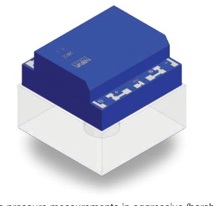
P1905
Backside Absolute
Pressure Sensor Die
The P1905 piezoresistive sensor die is designed for absolute pressure measurements in aggressive (harsh) media. The die has a reference vacuum chamber formed by hermetic low-stress bonding of silicon cap to the top side of device wafer. By applying pressure from backside of the die, P1905 sensor die eliminates the direct contact of sensor circuitry on top side with the applied media, which allows the P1905 die to mea sure pressure in aggressive liquids and gases. With NovaSensor’s SenStable® process, P1905 die features excellent long-term stability and repeatability (< 0.1% / year typ.).
Applications
- Automotive systems
- Process control systems
- Aerospace
- Pressure measurements in aggressive media
Amphenol
Advanced Sensors
Features
- Harsh media compatible
- Highly reliable, solid state silicon absolute pres sure sensor die pressurized from cavity side
- Recommended pressure ranges: 0…100 PSIA to 0…300 PSIA
- Die dimensions (L x W x H): 1.93 mm x 1.93 mm x 1.64 mm
- Bond pads all on same side for easy application packaging
- Other pressure ranges available
Page 2
P1905 Specifications
Parameter
Value
Units Notes
General
0...100 to
Pressure Range
PSIA
0...300
Max. Overpressure
600
PSIA
Backside Burst Pressure >4000
PSI
6
Electrical @ 25°C Unless Noted
1
mA 10VDC
Excitation (DC)
Max.
5
Volt
5000 ± 20% Ω
Bridge Resistance
Environmental
Temperature Range
Operating
-40° to 150° °C
2
Storage
-55° to 160° °C
Mechanical
1.93 x 1.93 x
Dimensions
mm L x W x H
1.64
Bond Pad Dimensions 0.10 x 0.10
mm L x W
Media compatible with silicon and
Media Compatibility
borosilicate glass.
Performance Parameters (1)
Value
Units Notes
Zero Offset
± 10
mV/V
Sensitivity
0.107 ± 0.030 mV/V/psi
3
Pressure Linearity
± 0.2
% Span
4
Pressure Hysteresis
± 10
µV/V
5, 6
Temp. Coefficient of Zero 0.5 ± 3
µV/V/C
5, 6
Temp. Coefficient of
0.27
%/C
5, 6
Resistance Temp. Coefficient of
-0.19
%/C
5, 6
Sensitivity Thermal Hysteresis of
± 25
µV/V
5, 6
Zero
- All values measured at 25ºC and 5 V excitation, unless otherwise noted. Samples from each wafer are used to verify bridge resistance, offset, span, linearity and die performance in the temperature range between 0ºC and 70ºC. 2. Backside burst pressure and operating temperature for sensor utilizing P1905 die can be lower than corresponding parameters for the die. 3. Typical span is equal to 160 mV at 300 psi. 4. Best fit straight line. 5. Between 0ºC and 70ºC. 6. Typical value.
Amphenol
Advanced Sensors
Shipping and Handling
All wafers are shipped in protective containers. The wafers are sawn on sticky tape. All wafers are electrically probed and visually inspected. Electrical and visual rejects are marked with ink dots. Each wafer has the following information: part number, lot number, wafer number, and the number of good parts.
Warrants
NovaSensor® warrants its products against defects in material and workmanship for 12 months from the date of shipment. Products not subjected to misuse will be repaired or replaced. NovaSensor reserves the right to make changes without further notice to any products herein. NovaSensor makes no warranty, representation or guarantee regarding the suitability of its products for any particular application. NovaSensor does not assume any liability arising out of the application or use of any product or circuit and specifically disclaims, and all liability, with out limitation consequential or incidental damages. The foregoing warranties are exclusive and in lieu of all other
warranties, whether written, oral, implied or statutory. No implied statutory warranty of merchantability of fitness for a particular purpose shall apply.
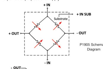
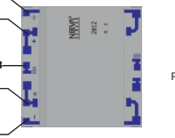
+ IN
+ IN SUB
P1905 Wire Bond
+ OUT
Diagram
- IN
Notes: Five (5) wire bonds are required. Both +IN and +IN SUB need to be connected to the highest potential in the circuitry.
www.amphenol-sensors.com
© 2016 Amphenol Corporation. All Rights Reserved. Specifications are subject to change without notice. Other company names and product names used in this document are the registered trademarks or trademarks of
their respective owners.