

 Download PDF
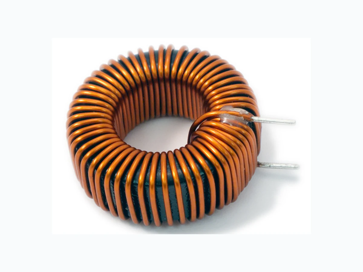
P1900 MPSIND
Document overview
- PDF pages: 1
Technical content
Page 1
PASSIVE POWER FACTOR
CORRECTION INDUCTORS
P1900 SERIES

Designed for use in off-line AC-DC pre-regulators circuits for
switching power converters applications
Low core loss and high flux density
Insulation class system: B (130°C), F (155°C) or H(180°C)
Dielectric Withstanding Voltage (DWV): 2KVRMS Operating Temperature: -20°C to +105°C
RoHS Compliant Product
Custom Design Available
| ELECTRICAL PARAMETERS @ 25°C | ||||||||||
|---|---|---|---|---|---|---|---|---|---|---|
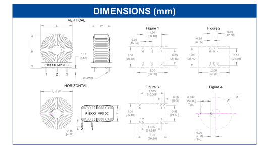
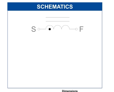
| Part Number | L T (μH MIN)1 | erminal3 (S-F) | DCR (mΩ MAX)1, 2 | I @ 80% L (ADC) | I @ 65% L (ADC) | I @ 50% L (ADC) | I @ 30% L (ADC) | Pins Dia. (Ø AWG) | LxWxH (in. MAX) | PCB Mounting Layout |
| P19000 | 240 | 1-5, 2-4 | 28 | 16.50 | 37.00 | 60.00 | 60.00 | 14 x 2 | 2.7x1.0x2.8 | V / Fig. 2 |
| P19001 | 290 | 1-5, 2-4 | 53 | 14.80 | 33.00 | 53.50 | 53.50 | 14 x 2 | 2.7x1.0x2.8 | V / Fig. 2 |
| P19002 | 400 | 1-5, 2-4 | 120 | 10.60 | 24.00 | 38.50 | 38.50 | 15 x 2 | 2.6x1.0x2.7 | V / Fig. 3 |
| P19003 | 440 | 1-5, 2-4 | 55 | 12.20 | 27.00 | 44.00 | 44.00 | 15 x 2 | 2.6x1.0x2.7 | V / Fig. 3 |
| P19004 | 440 | 1-5, 2-4 | 55 | 12.20 | 27.00 | 44.00 | 44.00 | 15 x 2 | 2.6x2.6x1.0 | H / Fig. 4 |
| P19005 | 490 | 1-5, 2-4 | 118 | 11.20 | 25.00 | 40.50 | 40.50 | 15 x 2 | 2.6x1.0x2.7 | V / Fig. 3 |
| P19006 | 500 | 1-5, 2-4 | 90 | 11.40 | 26.00 | 41.50 | 41.50 | 15 x 2 | 2.6x1.0x2.7 | V / Fig. 3 |
| P19007 | 820 | 2-5 | 95 | 7.50 | 17.00 | 27.00 | 27.00 | 14 | 2.7x1.0x2.8 | V / Fig. 1 |
| P19008 | 1600 | 2-5 | 241 | 6.40 | 14.00 | 23.00 | 23.00 | 15 | 2.7x1.0x2.8 | V / Fig. 1 |
| P19009 | 2000 | 2-5 | 286 | 5.70 | 13.00 | 20.50 | 20.50 | 15 | 2.7x1.0x2.8 | V / Fig. 1 |
- Test conditions: 10KHz, 1VRMS. 2. Combined resistance of the “x2” winding. 3. Only those assigned terminals will have the self-lead pins.
Product performance is limited to specified parameters. Data is subject to change without prior notice.
Tel: 310-325-1043 Fax: 310-325-1044
Unless otherwise specified, all tolerances are: inch: .XX : ±0.015 .XXX : ±0.004 mm: X,X : ±0,38 X,XX : ±0,10
www.mpsind.com sales@mpsind.com