
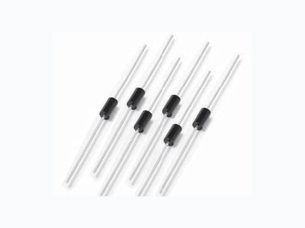
P0060LA LEIDITECH
Document overview
- Manufacturer or author: Provided By www.digicamel.com(FREE DATASHEET DOWNLOAD SITE)
- PDF pages: 9
Technical content
The L Series are designed to protect baseband equipment such as modems, line cards, CPE and DSL from damaging overvoltage transients. The series provides a cost-effective through-hole solution that enables equipment to comply with global regulatory standards. P0060~P3500LA_B_C Series Thyristor Surge Suppressors
Description
Electrical Characteristics
V DRM I DRM =5µA V S 100V/µS V T I T =2.2Amps I S I T I H Capacitance @1MHz, 2V bias V min V max V max mA max A max mA min pF min pF max P0060LA 6 15 4 800 2.2 50 25 50 P0080LA 6 25 4 800 2.2 50 25 50 P0300LA 25 40 4 800 2.2 50 55 70 P0640LA 58 77 4 800 2.2 150 40 60 P0720LA 65 88 4 800 2.2 150 35 55 P0900LA 75 98 4 800 2.2 150 35 55 P1100LA 90 130 4 800 2.2 150 30 60 P1300LA 120 160 4 800 2.2 150 25 40 P1500LA 140 180 4 800 2.2 150 25 40 P1800LA 170 220 4 800 2.2 150 25 30 P2300LA 190 260 4 800 2.2 150 25 30 P2600LA 220 300 4 800 2.2 150 25 30 P3100LA 275 350 4 800 2.2 150 20 30 P3500LA 320 400 4 800 2.2 150 20 30
- Low voltagr overeshoot
- Low on-state voltage
- Does not degrade with use
- Fails short circuit when surged in excess of ratings
- Low Capacitance Features and Benefits Applicable Global Standards
- TIA-968-A
- ITU K.20/21 Enhanced level*
- ITU K.20/21 Basic Level
- GR 1089 Inter building*
- GR 1089 Inter building
- IEC 6100-4-5
- YD/T 1082
- YD/T 993
- YD/T 950
Thyristor Surge Suppressors P0060~P3500LA_B_C Series Part Number V DRM I DRM =5µA V S 100V/µS V T I T =2.2Amps I S I T I H Capacitance @1MHz, 2V bias V min V max V max mA max A max mA min pF min pF max P0060LB 6 15 4 800 2.2 50 40 85 P0080LB 6 25 4 800 2.2 50 40 85 P0300LB 25 40 4 800 2.2 50 40 85 P0640LB 58 77 4 800 2.2 150 40 60 P0720LB 65 88 4 800 2.2 150 35 60 P0900LB 75 98 4 800 2.2 150 35 60 P1100LB 90 130 4 800 2.2 150 30 60 P1300LB 120 160 4 800 2.2 150 25 40 P1500LB 140 180 4 800 2.2 150 25 40 P1800LB 170 220 4 800 2.2 150 25 40 P2300LB 190 260 4 800 2.2 150 25 30 P2600LB 220 300 4 800 2.2 150 20 30 P3100LB 275 350 4 800 2.2 150 20 30 P3500LB 320 400 4 800 2.2 150 20 30 P0060LC 6 15 4 800 2.2 50 60 260 P0080LC 6 25 4 800 2.2 50 60 260 P0300LC 25 40 4 800 2.2 50 60 250 P0640LC 58 77 4 800 2.2 150 55 155 P0720LC 65 88 4 800 2.2 150 50 150 P0900LC 75 98 4 800 2.2 150 45 140 P1100LC 90 130 4 800 2.2 150 45 115 P1300LC 120 160 4 800 2.2 150 40 105 P1500LC 140 180 4 800 2.2 150 35 95 P1800LC 170 220 4 800 2.2 150 35 90 P2300LC 190 260 4 800 2.2 150 30 80 P2600LC 220 300 4 800 2.2 150 30 80 P3100LC 275 350 4 800 2.2 150 30 70 P3500LC 320 400 4 800 2.2 150 25 65 Notes: - Absolute maximum ratings measured at TA= 25ºC (unless otherwise noted). - Devices are bi-directional (unless otherwise noted) I PP I TSM 50/60 Hz di/dt0.2x310 0.5x700 2x10 2x10 8x20 1.2x50 10x160 10x160 10x560 10x560 5x320 9x720 10x360 10x360 10x1000 10x1000 5x310 10x700 A min A min A min A min A min A min A min A min A min A min A/µs max A 20 1501 50 90 50 75 75 45 75 20 500 B2 5 250 250 1501 00 1001 25 80 1002 55 00 C5 05 00 4002 00 1502 00 1751 00 2003 05 00 Notes:
1 Current waveform in µs
2 Voltage waveform in µs
- Peak pulse current rating (I PP ) is repetitive and guaranteed for the life of the product. - I PP ratings applicable over temperature range of -40ºC to +85ºC - The device must initially be in thermal equilibrium with -40°C < T J < +150°C
Thyristor Surge Suppressors P0060~P3500LA_B_C Series I H I T I S I DRM V DRM V T +V-V V S I H I T I S I DRM V DRM V T +V-V V S V-I Characteristics 100 t r t d Peak Value Half Value t – Time (µs) I PP – Peak Pulse Current – % I PP t r = rise time to peak v alue t d = decay time to half v alue Waveform = t r x t d t r x t d Pulse Wave-form -40- 20 02 04 06 08 01 00 1201 40 160 Junction Temperature (T J Percent of V S Change – % Normalized V S Change versus Junction Temperature 0.4 -40- 20 02 04 06 08 01 00 1201 40 160 0.6 0.8 1.0 1.2 1.4 1.6 1.8 2.0 Case Temperature (T C Ratio of I H I H C Normalized DC Holding Current versus Case Temperature
Thyristor Surge Suppressors P0060~P3500LA_B_C Series tinUeulaVretemaraPlobmySegakcaP DO-15 T J Operating Junction Temperature Range T S Storage Temperature Range R JA Thermal Resistance: Junction to Ambient 60 °C/W Thermal Considerations Time erutarep meT T P T L T S(max) T S(min) t P t L t S time to peak temperature (t 25ºC to peak) Ramp-down Ramp-up Preheat Critical Zone T L to T P Figure 1 Soldering Parameters Pb-Free assembly (see Fig. 1) Pre Heat - Temperature Min (T s(min) - Temperature Max (T s(max) - Time (Min to Max) (t s 60-180 secs. Average ramp up rate (Liquidus Temp (T L to peak) 3°C/sec. Max. T S(max) to T L - Ramp-up Rate 3°C/sec. Max. - Temperature (T L ) (Liquidus) - Temperature (t L 60-150 secs. Peak Temp (T P Time within 5°C of actual Peak Temp (t p ) 30 secs. Max. Ramp-down Rate 6°C/sec. Max. Time 2 5°C to Peak Temp (T ) 8 min. Max.
Figure 5. Test circuit 3 for dynamic I 1/ Adjust the current level at the Iv alue by short circuiting the AK of the D.U.T. 3/ The D.U.T.w ill come back off-state within 50ms maximum.
Thyristor Surge Suppressors P0060~P3500LA_B_C Series Lead Material Copper Alloy Terminal Finish 100% Matte-Tin Plated Body Material High T emp V olta ge Blo ck ing 80% Rated V DRM AC P eak 504 or 10 08 hrs. MIL -S TD-750 (Method 10 40) JEDEC, JESD22-A- 10 1 T emp Cy cling cy cles. MI L- ST D-750 (Method 1 051) EIA/JEDEC, JESD22-A 10 4 Biased T emp & Humidity 52 V DC JEDEC, JESD22-A- 10 1 High Te mp St or ag e JEDEC, JESD22-A- 10 1 Lo w T emp S to ra ge -65°C, 1 0 08 hrs. Ther mal Sho ck 1 0 cy cles. MI L- S TD-750 (Method 1 056) JEDEC, JESD22-A- 10 6 Au t ocl av e (Pr essu re Cook er T est) JEDEC, JESD22-A- 10 2 Resistance t o Solder Heat Mois tu r e Sensitivity Le ve l Pa r t Ma rk ing Pa r t Number ing CONSTRUCTION VA RIABL E REEL PACK I PP RATING RoHS COMPLIANT T YPE P = SIDACtor P x L RP MED IA N VOL TA GE PACKAGE TYPE xx x0 G Pxxxx Pa r t Marking Code (R efer to Electrical Characteristics T able) Dimensions — DO-15 L LG D B Dimension Inc hes Millimeters MI NM AX MIN MAX B 0.028 0.034 0.7 11 0.864 D 0.1 2 0.1 4 3.048 3.556 G 0.235 0.27 5.969 6.858 L4 .521 Pa ck ing Options Pa ck age T ype Description Quantity Added Industry Standard G DO -1 5 Axial T ape & R eel 20 00 RP EIA-R S- 296-D Spacing off center, either side 0.039 (1.0) B C A D E recess depth max 0.7 5” 2.55 (64.8) TY P 3.15 (80.0) T YP Dimensions are in inches (and millimeters). Direction of Feed G S ymbols Descriptio nI nc hes MM A Component Spacing (lead to lead) 5.08 ± 0.508 B Inner T ape Pit ch 52.37 ± 1 .498 CT ape W idth 6.35 D Max. O ff Alignment 1 .21 9 ER eel Dimension 330.2 F Max. Hub R ecess 7 6.1 9 G Max. Abor Hole 17 .27
Thyristor Surge Suppressors P0060~P3500LA_B_C Series Phone: +86- 021-50827201 Email:sale1@leiditech.com http://www.leiditech.com SHANGHAI LEIDITECH ELECTRONICS TECHNOLOGY CO., LTD