
MTPT75_17 NELLSEMI
Document overview
- Manufacturer or author: Provided By www.digicamel.com(FREE DATASHEET DOWNLOAD SITE)
- PDF pages: 5
Technical content
FEATURES
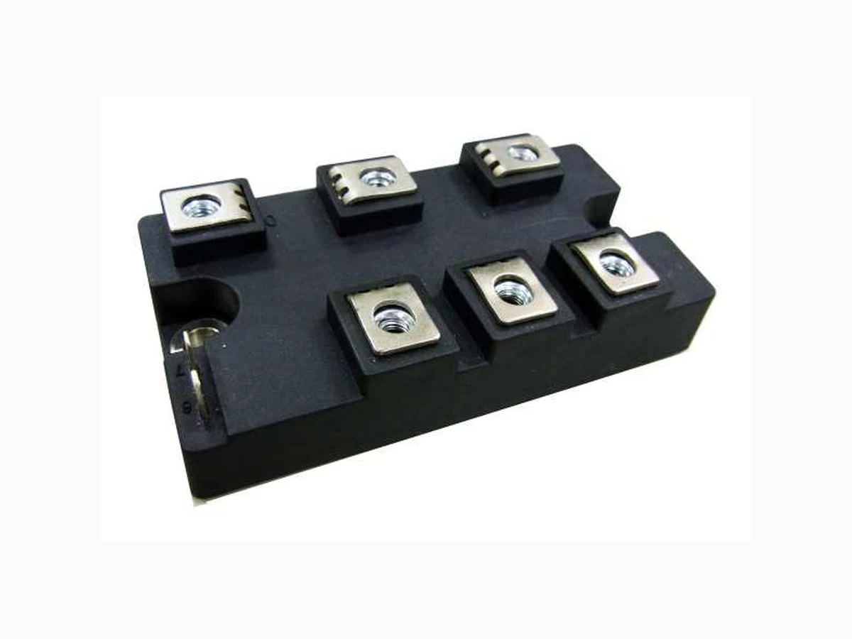
UL recognition file number E320098 Small volume, light weight Three-phase bridge and a thyristor Epoxy meets UL 94 V-O flammability rating PRIMARY CHARACTERRISTICS IF(AV) Weight: 210g (7.4 ozs) 75A VRRM 800V to 1600V 1.3V/1.6V 20 µA 150ºC I /IFSM TSM IR V /VFM TM RoHS RoHS Three-Phase Bridge + Thyristor, 75A Nell High Power Products Compliant to RoHS High surge current capability Low thermal resistance Small thermal resistance ADVANTAGE TJ max. 750A/920A MTPT7508 Thru MTPT7516 Isolation voltage up to 2500V International standard package All dimensions in millimeters
Applications
lnverter for AC or DC motor control Current stablilzed power supply Switching power supply 2- 5.5 6-M5 SCREWS 30 2032 93.5MAX 2020 50.5 M AX 22MAX 294 + -R2 G K Page 1 of 5www.nellsemi.com 4 3 0 1 2 (0) ( 1) ( 2) (3)(4)(5) (7) (6) MTPT75 Series Glass passivated chip junction
MAJOR RATINGS AND CHARACTERISTICS (T = 25°C unless otherwise noted)A PARAMETER V V SYMBOL MTPT75 UNIT 900 1300 800 1200 1600 12 16 1700 Maximum repetitive peak reverse voltage Peak reverse non-repetitive voltage Peak forward surge current single sine-wave superimposed on rated load Rating (non-repetitive, for t greater than 1 ms and less than 8.3 ms) for fusing Operating junction temperature range V /VRRM RRM VRSM IFSM 2I t 281 0 -40 to 150 750 2A s A A ºC ELECTRICAL CHARACTERISTICS (T = 25°C unless otherwise noted)A PARAMETER V µA SYMBOL MTPT75 UNIT 08 12 16 Maximum instantaneous forward drop per diode Maximum reverse DC current at rated DC blocking VF IR 1.3 voltage per diod TEST CONDITIONS I = 75AF T = 25°CA T = 150 °CA Storage temperature range TSTG -40 to 125 ºC TJ mA Maximum Ratings for Diodes Output DC current three-phase full wave, T = 100 °Cc IO SWITCHING SYMBOL TEST CONDITIONS VALUES Typical delay time Typical rise time td tr TJ = 25 °C ,gate current = 1A dl /dt = 1 A/µsg Typical tum-off time tq I = 300A ; dl/dt = 15 A/ µs ; T = T maximum,TM J J V = 50V ; dV/dt = 20V/µs ; gate 0V ,100Ω R μs 50 to 150 UNITS V = 0.67 Vd DRM Page 2 of 5www.nellsemi.com RoHS RoHS Nell High Power Products ºC/W ºC/W Thermal Impedance, junction to case RthJC 0.25 Thermal Impedance, case to heatsink RthCS 0.10 FORWARD CONDUCTION SYMBOL TEST CONDITIONS Maximum average on-state current at case temperature IT(AV) 180° conduction, half sine wave ,50Hz AMaximum peak, one-cycle, on-state non-repetitive surge current ITSM t = 10 ms No voltage reapplied Sine half wave, initial TJ = TJ maximum t = 8.3 ms Maximum I2t for fusing I 2t 2A s Maximum I2√t for fusing I 2√t t = 0.1 ms to 10 ms, no voltage reapplied Maximum on-state voltage drop VTM ITM = 225A , TJ = 25 °C, 180° conduction Maximum holding current IH Anode supply = 6 V, initial IT = 30 A, TJ = 25 °C mA Maximum latching current IL Anode supply = 6 V 400 V UNITSVALUES 920 810 4230 3865 42.3 1.6 150 A t = 10 ms t = 8.3 ms t = 10 ms t = 8.3 ms 2kA √ 3005 2725reapplied 100%V RRM t = 10 ms t = 8.3 ms reapplied 100%V RRM No voltage reapplied 965 775 PARAMETER Gate pulse: 10 V, 100 μs, TJ = 25 °C Maximum Ratings for Thyristor s PARAMETER MTPT75 Series
SYMBOL TEST CONDITIONS VALUES UNITS Maximum peak gate power PGM t p 5 ms, TJ = TJ maximum W Maximum average gate power PG(AV) f = 50 Hz, TJ = TJ maximum Maximum peak gate current IGM t p 5 ms, TJ = TJ maximum A Maximum peak negative gate voltage - VGT 10 V gate voltage to trigger VGT Anode supply = 6V, resistive load; Ra = 1 TJ = 25 °C IGT mA Maximum gate voltage that will not trigger VGD TJ = TJ maximum, 67% VDRM applied 0.25 Maximum gate current that will not trigger IGD mA Maximum rate of rise of turned-on current dI/dt TJ = 125ºC, V = 0.5V , I = 100 mA,D DRM G A/μs THERMAL AND MECHANICAL SPECIFICATIONS SYMBOL TEST CONDITIONS VALUES UNITS junction operating and storage temperature range T TJ stg, - 40 to 125 °C Maximum thermal resistance, junction to case per junction RthJC DC operation °C/WTypical thermal resistance, case to heatsink per module RthCS Mounting surface, smooth , flat and greased Mounting torque ± 10 % to heatsink, M5 A mounting compound is recommended and the torque should be rechecked after a period of about 3 hours to allow for the spread of the compound. to terminal, M5 Approximate weight 210 7.4 TRIGGERING J J J = TJ J J - VGT Maximum required DC a ΩMaximum required DC gate current to trigger thCS 150 V oz. g 0.10 0.40 BLOCKING TEST CONDITIONS Maximum peak reverse and off-state leakage current IRRM, IDRM TJ = 125 °C RMS isolation Voltage VISO
50 Hz, circuit to base,
all terminals shorted, 25 ºC ,60s V Critical rate of rise of off-state voltage dV/dt TJ = TJ maximum, exponential to 67 % rated VDRM V/μs 500 mA 2500 UNITS N.m 150 Device code 75 16MTPT 321 2 - I rating : "75" for 75AF(AV)
3 RRM- Voltage code : code x 100 = V
Module type : “MTPT” for 3 i iØ Br dge + Thyr stor Page 3 of 5www.nellsemi.com RoHS RoHS Nell High Power Products PARAMETER SYMBOL VALUES dI /dt = 0.1 A/µsG PARAMETER PARAMETER MTPT75 Series
Fig.1 Power dissipation 756045 Three phase 0 150 Fig.2 Forward current derating curve 10050 Three phase 0.40 0.20 Fig.3 Transient thermal impedance 100101.00.10.01 Zth(j-C) 1000 500 Fig.4 Max non-repetitive forward surge current 100 10 50HZ Per one element Single phase half wave T =25j °C start 0.5 1.0 1000 100 Fig.5 Forward characteristics 2.01.5 2.5 T =25J °C max. 100 Fig.6 SCR power dissipation 7560453015 Page 4 of 5www.nellsemi.com RoHS RoHS Nell High Power Products P (W)vtot (For Diodes) I (A)D (For Diodes) T (°C)c IF(AV), (A) °C/W t (S) (For Diodes) 0.001 (For Diodes) I (A)FSM Cycles (For Diodes) V (V)F I (A)F P (W)TAV I (A)F MTPT75 Series
Fig.7 SCR forward current derating curve 10050 0.001 0.50 0.25 Fig.8 SCR transient thermal impedance 100101.00.10.01 Zth(j-C) 0.5 1.0 1000 100 Fig.9 SCR forward characteristics 2.52.01.5 max. T =25j °C max. Page 5 of 5www.nellsemi.com RoHS RoHS Nell High Power Products I (A)T(Av), T (°C)c Time (S) °C/W I (A)T, V (V)TM PeakGatePower(10W) Average Gate Power(3W) 110 Peak Forward Gate Voltage (10V) 0.1 Maximum Gate Non-Trigger Voltage 25°C -40°C 125°C Peak Gate Current (3A) Fig.10 Gate trigger characteristics 210 310 410 010 110 210 I (mA)G V (V)G MTPT75 Series