
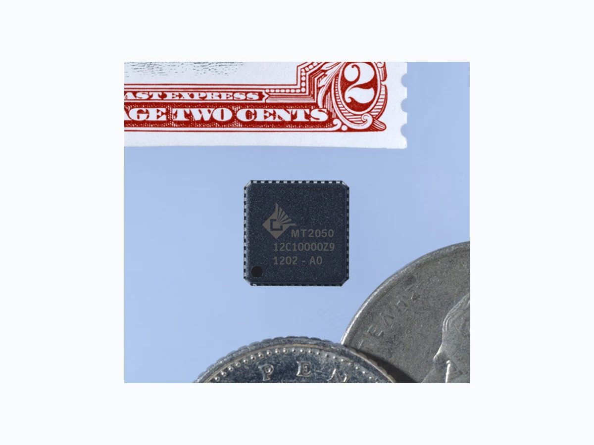
MT2050 ETC1
Document overview
- Manufacturer or author: Provided By www.digicamel.com(FREE DATASHEET DOWNLOAD SITE)
- PDF pages: 2
Technical content
MT2050 SINGLE-CHIP BROADBAND TUNER CABLE MODEM TUNER AND DIGITAL SET-TOP BOX APPLICATIONS Product Brief M I C R O T U N E™ Preliminary and Confidential The MT2050 is an advanced single-chip broadband tuner that has been optimized for high performance cable modems and digital cable STBs that require low composite distortion and noise under digital cable environments. The MT2050 includes all active circuitry required to implement total RF functionality, making it the world’s first complete RF/amplifier silicon front end. It is capable of receiving frequencies in the 48 MHz to 860 MHz range and converting a selected channel to a standard intermediate frequency (IF). Supported IF frequencies include NTSC, PAL, and digital standards including DOCSIS, EuroDOCSIS, DVB-C, and ITU J83, A, B, C. The MT2050’s low close-in phase noise allows it to be used for both digital and analog video signals including video, high speed data, and voice. Its dual- conversion architecture, with no requirement for tracking filters, yields the desirable characteristics of traditional cable television tuners: controlled input impedance across the entire input band, low in-band emissions, and outstanding image rejection.
APPLICATIONS
- Cable modems / voice- enabled cable modems
- Digital set-top boxes (STB)
- Home gateways
FEATURES
- 48 MHz to 860 MHz input frequency range
- Works seamlessly with all analog and digital demodulators
- Low power dual-conversion architecture
- Minimal external components
- No manually tunable parts required
- Simple interface to external filters
- Integrated IF variable gain amplifier for direct connection to digital demodulators
- Fully compatible with NTSC, PAL, SECAM, DAVIC, DVB-C, DOCSIS 1.0, 1.1 and 2.0, EuroDOCSIS and other standards MT2050 Tuner
MT2050 SINGLE-CHIP BROADBAND TUNER C ABLE MODEM TUNER AND PRODUCT BRIEF D IGITAL SET-TOP BOX APPLICATIONS PB-00038 Rev 1.0 — April 2002 Page 2 of 2 Preliminary and Confidential PIN DIAGRAM VLNAin 1 VCClna 2 DAGCin 3 AVCClo1 4 LO1tk1 5 LO1tk2 6 LO1reg 7 DVCClo1 8 LO1lpf 9 GPO0 10 DNC 11 SERca 12 SERen 13 SERscl 14 SERsda 15 DNC 16 VCC 17 SROn 18 SROp 19 GPADin 20 VGAop 21 VGAon 22 VCCvga 23 VGActrl 24
25 VGAin
26 VGAip
27 DNC
28 GPO1
29 DVCClo2
30 DNC
31 LO2lpf
32 LO2reg
33 LO2tk
34 AVCClo2
35 FGAon
36 FGAop
37 DNC
38 VCCfga
39 VCCmx2
40 MIX2in
41 MIX2ip
42 DNC
43 VCCmx1
44 MIX1op
45 MIX1on
46 GPO2
47 VCClna
48 VLNAip
RECOMMENDED OPERATING CONDITIONS PARAMETER M IN TYP M AX U NIT Input frequency range 48 860 MHz First intermediate center frequency 1220 MHz Second intermediate center frequency (programmable) 30 60 MHz Supply voltage 4.75 5 5.25 V Supply voltage ripple 15 mV Operating junction temperature 100 °C VGA output load impedance 300 Ω Serial control clock 400 kHz ABSOLUTE MAXIMUM RATINGS PARAMETER M IN M AX U NIT Supply voltage 6 V Storage temperature range -40 +150 °C Lead temperature (soldering, 4 seconds) +245 °C Input voltage -0.3 VCC +0.3 V
ELECTRICAL CHARACTERISTICS
PARAMETER M IN TYP M AX U NIT Power Supply Active current 325 mA Shut-down current 40 mA Upconversion Input frequency range 48 860 MHz Return loss 9.5 dB First IF center frequency 1220 MHz Noise figure, max gain 7 dB Terminal voltage gain 18 dB AGC range 30 dB Gain variation at any frequency -3 +3 dB OIP3 68 72 dBmV Downconversion Input frequency range 1220 MHz Noise figure 10 dB Terminal voltage gain 29 dB Image rejection 28 33 dBc OIP3 77 79 dBmV LO1 LO frequency 1268 2080 MHz LO step size 1 kHz Phase noise (10 kHz) -86 dBc/Hz Phase noise (100 kHz) -109 dBc/Hz Spurious -60 dBc LO2 LO frequency 1160 1190 MHz LO step size 50 kHz Phase noise (10 kHz) -94 dBc/Hz Phase noise (100 kHz) -114 dBc/Hz Spurious -60 dBc IF VGA Frequency range 30 60 MHz Output voltage 1.0 Vp-p Terminal voltage gain 12.5 51.5 dB Noise figure, max gain 12.5 dB OIP3 76 dBmV Serial Interface Serial clock frequency 400 kHz VIH 2.3 V VIL 1.5 V Worldwide Headquarters • Microtune, Inc., 2201 Tenth Street, Plano, TX 75074, USA • Tel: +1-972-673-1600, Fax: +1-972-673-1602, E-mail: sales@microtune.com, Web site: www.microtune.com For a detailed list of design centers, sales offices, and sales representatives, visit our Web site at www.microtune.com. The information in this document is believed to be accurate and reliable. Microtune assumes no responsibility for any consequences arising from the use of this information, nor from any infringement of patents or the rights of third parties which may result from its use. No license is granted by implication or otherwise under any paten t or other rights of Microtune. The information in this publication replaces and supersedes all information previously supplied, and is subject to change without notice. The customer is responsible for assuri ng that proper design and operating safeguards are observed to minimize inherent and procedural hazards. Microtune assumes no responsibility for applications assistance or customer product design. The devices described in this document are not authorized for use in medical, life-support equipment, or any other application involving a potential risk of severe property or environmental damage, personal injury, or death without prior express written approval of Microtune. Any such use is understood to be entirely at the user’s risk. Microtune, MicroTuner, MicroStreamer, VideoCaster, and the Microtune logo are trademarks of Microtune, Inc. All other trademarks belong to their respective companies. Microtune’s products are protected by one or more of the following U.S. patents: 5,625,325; 5,648,744; 5,717,730; 5,737,035; 5, 739,730; 5,805,988; 5,847,612; 6,100,761; 6,104,242; 6,144,402; 6,163,684; 6,169,569; 6,177,964; 6,218,899 and additional patents pending or filed. Entire contents Copyright © 2002 Microtune, Inc.