


 Download PDF
MMBD4148SE - Small Signal Diode
Document overview
- PDF pages: 8
Technical content
Page 1
Small Signal Diode
MMBD4148SE, MMBD4148CC, MMBD4148CA
Features
- These are Pb-Free Devices
MAXIMUM RATINGS (TA = 25 °C unless otherwise noted)
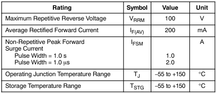
Stresses exceeding those listed in the Maximum Ratings table may damage the
DATA SHEET
3
1 2
SOT-23 (TO-236)
CASE 318-08
MARKING DIAGRAM
DxM ? ?
1
Dx = Device Code x = 4, 5, 6 M = Assembly Operation Month ? = Pb-Free Package (Note: Microdot may be in either location)
CONNECTION DIAGRAMS
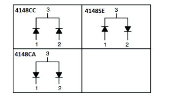
device. If any of these limits are exceeded, device functionality should not be assumed, damage may occur and reliability may be affected.
THERMAL CHARACTERISTICS (TA = 25 °C unless otherwise noted)

ELECTRICAL CHARACTERISTICS (TA = 25 °C unless otherwise noted)
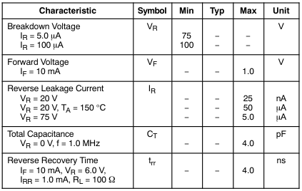
Product parametric performance is indicated in the Electrical Characteristics for the listed test conditions, unless otherwise noted. Product performance may not be indicated by the Electrical Characteristics if operated under different conditions.
© Semiconductor Components Industries, LLC,2004 October, 2026 − Rev. 4
ORDERING INFORMATION
See detailed ordering, marking and shipping information in the package dimensions section on page 4 of this data sheet.
Publication Order Number:
MMBD4148SE/D
Page 2
TYPICAL PERFORMANCE CHARACTERISTICS
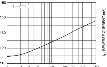
1 2 3 5 10 20 30 50
100
IR, REVERSE CURRENT (?A)
Figure 1. Reverse Voltage vs. Reverse Current
BV − 1.0 to 100 ?A
1 2 3 5 10 20 30 50
100
IF, REVERSE CURRENT (?A)
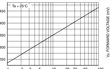
Figure 3. Forward Voltage vs. Forward Current
VF − 1.0 to 100 ?A
100 200 300 500
10 20 30 50
IF, FORWARD CURRENT (mA)
Figure 5. Forward Voltage vs. Forward Current
VF − 10 to 800 mA
10
20 30
70 100
50
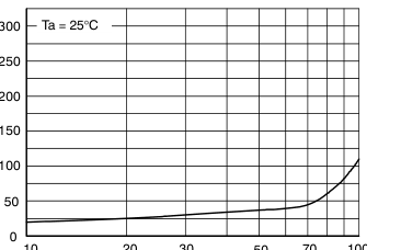
VR, REVERSE VOLTAGE (V) Figure 2. Reverse Current vs. Reverse Voltage
IR − 10 to 100 V
0.1 0.2 0.3 0.5
1 2 3 5 10
IF, FORWARD CURRENT (mA)
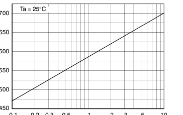
Figure 4. Forward Voltage vs. Forward Current
VF − 0.1 to 10 mA
6 8
12 14
0 2 4
10
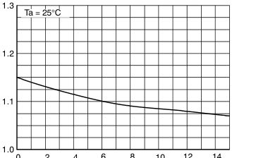
REVERSE VOLTAGE (V)
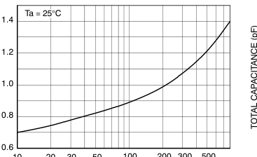
Figure 6. Total Capacitance vs. Reverse Voltage
Page 3
TYPICAL PERFORMANCE CHARACTERISTICS (Continued)
10 20 30 40 50 60
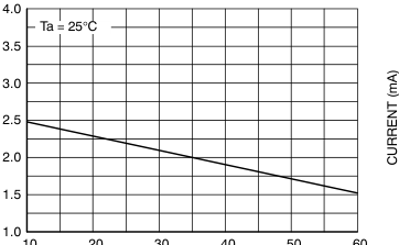
REVERSE CURRENT (mA)
Figure 7. Reverse Recovery Time vs. Reverse Current
TRR − IR 10 mA to 60 mA
0 50 100 150 200
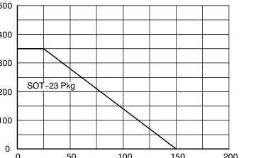
IO, AVERAGE TEMPERATURE (°C) Figure 9. Power Derating Curve
0
50
100
150
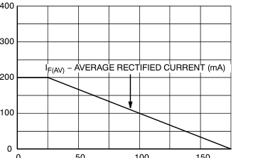
TA, AMBIENT TEMPERATURE (°C) Figure 8. Average Rectified Current (IF(AV)) vs. Ambient Temperature (TA)
Page 4
ORDERING INFORMATION
| Column 1 | Column 2 | Column 3 | Column 4 |
|---|---|---|---|
| Device | Specific Marking Code | Package | Shipping† |
| MMBD4148SE MMBD4148SE-NC | D4 | SOT-23 (Pb-Free) | 3,000 / Tape & Reel |
| MMBD4148CC MMBD4148CC-NC | D5 | ||
| MMBD4148CA MMBD4148CA-NC | D6 |
† For information on tape and reel specifications, including part orientation and tape sizes, please refer to our Tape and Reel Packaging Specifications Brochure, BRD8011/D. \* S, V and NSV Prefix for Automotive and Other Applications Requiring Unique Site and Control Change Requirements; AEC-Q101 Qualified and PPAP Capable.
Page 5
REVISION HISTORY
| Revision | Description of Changes | Date |
|---|---|---|
| 4 | Added “-NC” OPNs to order table. | 10/5/2026 |
This document has undergone updates prior to the inclusion of this revision history table. The changes tracked here only reflect updates made on the noted approval dates.
Page 6
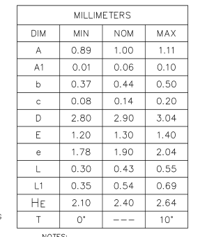
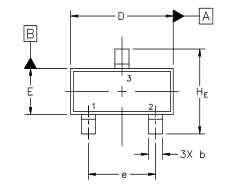
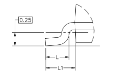
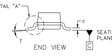
MECHANICAL CASE OUTLINE
PACKAGE DIMENSIONS
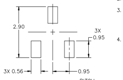
SOT−23 (TO−236) 2.90x1.30x1.00 1.90P
CASE 318 ISSUE AU
DATE 14 AUG 2024
SCALE 4:1
GENERIC
MARKING DIAGRAM\*
XXXM? ?
1
XXX = Specific Device Code M = Date Code ? = Pb−Free Package
\*This information is generic. Please refer to device data sheet for actual part marking. Pb−Free indicator, “G” or microdot “?”, may or may not be present. Some products may not follow the Generic Marking.
STYLES ON PAGE 2
| Column 1 | Column 2 | Column 3 | Column 4 |
|---|---|---|---|
| DOCUMENT NUMBER: | Electron 98ASB42226B Printed | ic versions are uncontrolled except when accessed directly from the Document Repository. versions are uncontrolled except when stamped “CONTROLLED COPY” in red. | |
| DESCRIPTION: | SOT−23 (TO−236) 2.90x1.30x1.00 1.90P | PAGE 1 OF 2 |
onsemi and are trademarks of Semiconductor Components Industries, LLC dba onsemi or its subsidiaries in the United States and/or other countries. onsemi reserves the right to make changes without further notice to any products herein. onsemi makes no warranty, representation or guarantee regarding the suitability of its products for any particular purpose, nor does onsemi assume any liability arising out of the application or use of any product or circuit, and specifically disclaims any and all liability, including without limitation special, consequential or incidental damages. onsemi does not convey any license under its patent rights nor the rights of others.
© Semiconductor Components Industries, LLC, 2019
Page 7
SOT−23 (TO−236) 2.90x1.30x1.00 1.90P
CASE 318
ISSUE AU
STYLE 6:
STYLE 7:
STYLE 1 THRU 5:
PIN 1. BASE
PIN 1. EMITTER
CANCELLED
- EMITTER
- BASE
- COLLECTOR
- COLLECTOR
STYLE 9:
STYLE 10:
STYLE 11:
PIN 1. ANODE
PIN 1. DRAIN
PIN 1. ANODE
- ANODE
- SOURCE
- CATHODE
- CATHODE
- GATE
- CATHODE−ANODE
STYLE 15:
STYLE 16:
STYLE 17:
PIN 1. GATE
PIN 1. ANODE
PIN 1. NO CONNECTION
- CATHODE
- CATHODE
- ANODE
- ANODE
- CATHODE
- CATHODE
STYLE 22:
STYLE 21:
STYLE 23:
PIN 1. RETURN
PIN 1. GATE
PIN 1. ANODE
- OUTPUT
- SOURCE
- ANODE
- INPUT
- DRAIN
- CATHODE
STYLE 27:
STYLE 28:
PIN 1. CATHODE
PIN 1. ANODE
- CATHODE
- ANODE
- CATHODE
- ANODE
DATE 14 AUG 2024
STYLE 8: PIN 1. ANODE 2. NO CONNECTION 3. CATHODE
STYLE 12:
STYLE 13:
STYLE 14:
PIN 1. CATHODE
PIN 1. SOURCE
PIN 1. CATHODE
- CATHODE
- DRAIN
- GATE
- ANODE
- GATE
- ANODE
STYLE 18:
STYLE 19:
STYLE 20:
PIN 1. NO CONNECTION PIN 1. CATHODE
PIN 1. CATHODE
- CATHODE
- ANODE
- ANODE
- ANODE
- CATHODE−ANODE
- GATE
STYLE 24:
STYLE 25:
STYLE 26:
PIN 1. GATE
PIN 1. ANODE
PIN 1. CATHODE
- DRAIN
- CATHODE
- ANODE
- SOURCE
- GATE
- NO CONNECTION
| Column 1 | Column 2 | Column 3 | Column 4 |
|---|---|---|---|
| DOCUMENT NUMBER: | 98ASB42226B | Electronic versions are uncontrolled except when accessed directly from the Document Repository. Printed versions are uncontrolled except when stamped “CONTROLLED COPY” in red. | |
| DESCRIPTION: | SOT−23 (TO−236) 2.90x1.30x1.00 1.90P | PAGE 2 OF 2 |
onsemi and are trademarks of Semiconductor Components Industries, LLC dba onsemi or its subsidiaries in the United States and/or other countries. onsemi reserves the right to make changes without further notice to any products herein. onsemi makes no warranty, representation or guarantee regarding the suitability of its products for any particular purpose, nor does onsemi assume any liability arising out of the application or use of any product or circuit, and specifically disclaims any and all liability, including without limitation special, consequential or incidental damages. onsemi does not convey any license under its patent rights nor the rights of others.
© Semiconductor Components Industries, LLC, 2019
Page 8

ADDITIONAL INFORMATION
TECHNICAL PUBLICATIONS:
ONLINE SUPPORT: www.onsemi.com/support
Technical Library: www.onsemi.com/design/resources/technical−documentation
For additional information, please contact your local Sales Representative at www.onsemi.com/support/sales
onsemi Website: www.onsemi.com