Read the Inchange Semiconductor ... document online.
MEK150-04DA ISC
Document overview
PDF pages: 3
Technical content
Page 1
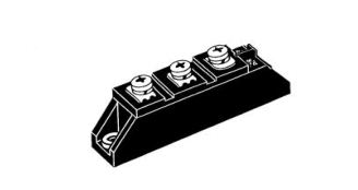
Fast Recovery Diode Module
DESCRIPTION
International standard packagewith DCB ceramic base plate
Planar passivated chips
Short recovery time
Low switching losses
SYMBOL
PARAMETER
VALUE
UNIT
VR
Diode reverse voltage,T=25℃ J
400
V
IF
DC current,T =100℃,rectangular, d = 0.5 C
150
A
IFpuls
Pulsed diode current, T = 45℃; t = 10 ms (50 Hz), sine VJ
1200
A
P D
Power dissipation per diode,T =25℃ C
260
W
T J
Junction Temperature
-40~150
℃
Tstg
Storage Temperature Range
-40~150
℃
V isol
Insulation test voltage, t = 1min
3600
V
THERMAL CHARACTERISTICS
SYMBOL
PARAMETER
MAX
UNIT
Rth j-c
Thermal Resistance,Junction to Case
0.35
℃/W
Page 2
Fast Recovery Diode Module
ELECTRICAL CHARACTERISTICS
SYMBOL
PARAMETER
CONDITIONS
MIN
TYP
MAX
UNIT
V F
Diode Forward Voltage
I =300A; T =25℃ F C
--
--
1.6
V
I =300A; T =150℃ F C
--
--
1.4
I R
Reverse current
V =400V;T=25℃ R J
--
--
2.0
mA
V =400V;T=150℃ R J
--
--
8.5
M
Mounting torque with screw M5
2.5
--
4
Nm
M
Terminal connection torque
2.5
--
4
Nm
Page 3
Fast Recovery Diode Module
Product Disclaimer
ISC reserves the rights to make changes of the content herein the datasheet at any time without notification. The information contained herein is presented only as a guide for the applications of our products.
MEK150-04DA is listed in the IC category. Available datasheets include documents from IXYS Corporation. DigiCamel provides a local PDF and searchable HTML technical text for online reference.
Summary
Fast Recovery Diode Module
Description
Fast Recovery Diode Module
Source titleMEK150-04DA Datasheet(PDF) - Inchange Semiconductor Company Limited



 Download PDF