
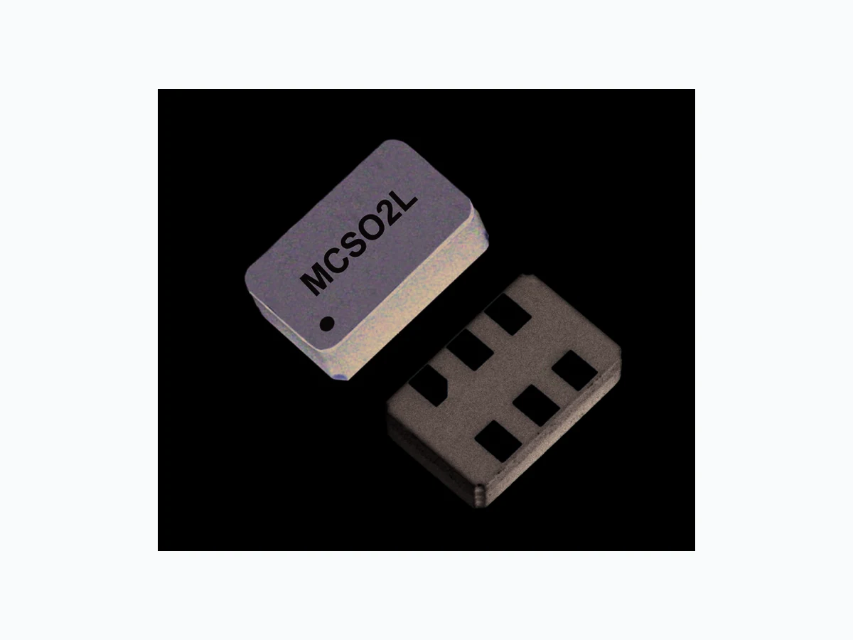
MCSO2L MICROCRYSTAL
Document overview
- Manufacturer or author: Provided By www.digicamel.com(FREE DATASHEET DOWNLOAD SITE)
- PDF pages: 2
Technical content
MCSO2L family package 5×3.2 mm From 40 MHz to 130 MHz LVDS Output Recommended Solder Pad: All dimensions in mm typical ELECTRICAL CHARACTERISTICS AT +25°C Frequency stability (standard) Over temperature range (see orderding info) Including: adjustment at 25°C long term aging 10 years over supply voltage ±5% ΔF/F ≤ ± 100 ppm Frequency stability version T Over temperature range (see ordering info) Including: adjustment at +25°C long term aging 1 year over supply voltage ±5% ΔF/F ≤ ± 50 ppm Supply voltage ± 5% 1)* Vdd 2.5 / 3.3 V Input current Idd see table 1 Output signal (load 100 ohm) LVDS Symmetry (max) 45 / 55 % Rise & fall time (20% to 80%) <1 ns Level Logic low (Typ/min) 1.1 / 0.9 V Level Logic high (Typ/max) 1.4 / 1.6 V Start-up time t <5 ms Jitter RMS (1KHz to 1MHz) <0.3 ps 100% Leadfree, RoHScompliant: DESCRIPTION: This SMD oscillator in ceramic package has been specially designed for surface mount using infrared, vapor phase or epoxy techniques. APPLICATIONS: - Avionics - Airborne equipments - Remote control - Security application - Radio Transceiver - Microprocessor clocks The MCSO2L's are supplied on trays (128 pcs / tray) For pick-and-place equipment, the parts are available in 12mm tapes with 250 parts min 1000 parts min SMT LVDS Clock oscillator in ceramic package Fundamental quartz mode frequency High shock and vibration resistance Wide temperature range Low aging Ultra low internal MSL Very fast start-up Excellent solderability Swiss made quality Customer specification on request 5.00 2.35 0.65 3.201.2 0.9 1 2 3 6 5 4 6 5 4 1 2 3 1.6 0.8 1.4 pin 1 E/D pin 2 NC pin 3 GND pin 4 Fout pin 5 CFout pin 6 Vdd Package: Bottom view * 1) C = 47nF ceramic must be connected between GND & Vdd differential Phase noise typical at 100MHz Static conditions 10Hz BW = 1Hz 100Hz 1 kHz 10 kHz 100kHz -70 -100 -125 -145 -150 dBc/ Hz
Version 3.0/05.2017 Micro Crystal AG Tel. +41 32 655 82 82 Mühlestrasse 14 Fax +41 32 655 82 83 CH-2540 Grenchen sales@microcrystal.com Switzerland www.microcrystal.com W = Vdd 2.5V V = Vdd 3.3V T = ±50ppm Blank = ±100ppm A = 0 to 70°C B = -40 to 85°C C = -55 to 125°C X = custom Frequency ENVIRONMENTAL CHARACTERISTICS: Storage temp. range -65 to +125°C Vibration resistance (survival) 10 to 2000Hz / 50g Shocks resistance (survival) 5000g / 0.3ms / ½ sine TERMINATIONS AND PROCESSING: Reflow soldering (peak) +260°C / 10s max Package Ceramic 5 x 3.2 x 1.6mm Lids Ceramic Terminations option T3 on request with tinned Ag/Cu/Sn E/D option 1 on request Reaction time ˂ 1μs Pin 1 open → Pin 3 Clock H → Clock L → Low PRODUCT DESCRIPTION AND ORDERING INFORMATION: All specifications subject to change without notice. Frequency «MHz» 40 80 100 128 Other frequencies on request STANDARD FREQUENCIES: - No power E/D function (pin 1) before Vdd is setting on option 1 E/D enable / disable option 2 blank Au plated T3 = tinned customer spec N° MCSO2L V T - C 100MHz E/D T3 XXX Frequency F= 40MHz 100MHz 130MHz W =Vdd = 2.5V < 5mA < 10mA < 20mA V =Vdd = 3.3V < 10mA < 15mA < 25mA TAbLE 1: Idd (Without load) A unique part number will be generated for each product specification 20xxxx-EA00 xxx pcs (in ESD plastic tray) 200xxx-ML00 xxx pcs (in tape & reel, any quantity)