
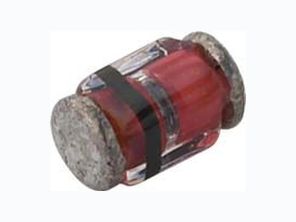
MCL4154_12 VISHAY
Document overview
- Manufacturer or author: Provided By www.digicamel.com(free datasheet download site)
- PDF pages: 4
Technical content
www.vishay.com Vishay Semiconductors Rev. 1.9, 01-Aug-12 1 Document Number: 85568 For technical questions within your region: DiodesAmericas@vishay.com, DiodesAsia@vishay.com, DiodesEurope@vishay.com THIS DOCUMENT IS SUBJECT TO CHANGE WITHOUT NOTICE. THE PRODUCTS DESCRIBED HEREIN AND THIS DOCUMENT ARE SUBJECT TO SPECIFIC DISCLAIMERS, SET FORTH AT www.vishay.com/doc?91000 Small Signal Fast Switching Diode MECHANICAL DATA Case: MicroMELF Weight: approx. 12 mg Cathode band color: black Packaging codes/options: TR3/10K per 13" reel (8 mm tape), 10K/box TR/2.5K per 7" reel (8 mm tape), 12.5K/box
FEATURES
- Silicon epitaxial planar diode
- Electrical data identical with the device 1N4154
- MicroMELF package
- AEC-Q101 qualified
- Material categorization: For definitions of compliance please see www.vishay.com/doc?99912
APPLICATIONS
- Extreme fast switches PARTS TABLE PART TYPE DIFFERENTIATION ORDERING CODE INTERNAL CONSTRUCTION REMARKS MCL4154 V RRM = 35 V MCL4154-TR3 or MCL4154-TR Single diode Tape and reel ABSOLUTE MAXIMUM RATINGS (Tamb = 25 °C, unless otherwise specified) PARAMETER TEST CONDITION SYMBOL VALUE UNIT Repetitive peak reverse voltage V RRM 35 V Reverse voltage V R 25 V Peak forward surge current t p = 1 μs I FSM 2A Repetitive peak forward current I FRM 450 mA Forward continuous current I F 200 mA Average forward current V R = 0 I FAV 150 mA Power dissipation P tot 500 mW THERMAL CHARACTERISTICS (Tamb = 25 °C, unless otherwise specified) PARAMETER TEST CONDITION SYMBOL VALUE UNIT Thermal resistance junction to ambient air Mounted on epoxy-glass hard tissue, Fig. 4, 35 μm copper clad, 0.9 mm copper area per electrode RthJA 500 K/W Junction temperature T j 175 °C Storage temperature range T stg - 65 to + 175 °C
www.vishay.com Vishay Semiconductors Rev. 1.9, 01-Aug-12 2 Document Number: 85568 For technical questions within your region: DiodesAmericas@vishay.com, DiodesAsia@vishay.com, DiodesEurope@vishay.com THIS DOCUMENT IS SUBJECT TO CHANGE WITHOUT NOTICE. THE PRODUCTS DESCRIBED HEREIN AND THIS DOCUMENT ARE SUBJECT TO SPECIFIC DISCLAIMERS, SET FORTH AT www.vishay.com/doc?91000 TYPICAL CHARACTERISTICS (Tamb = 25 °C, unless otherwise specified) Fig. 1 - Reverse Current vs. Junction Temperature Fig. 2 - Forward Current vs. Forward Voltage Fig. 3 - Diode Capacitance vs. Reverse Voltage Fig. 4 - Board for RthJA definition (in mm) ELECTRICAL CHARACTERISTICS (Tamb = 25 °C, unless otherwise specified) PARAMETER TEST CONDITION SYMBOL MIN. TYP. MAX. UNIT Forward voltage I F = 30 mA V F 1000 mV Reverse current VR = 25 V I R 100 nA VR = 25 V, Tj = 150 °C I R 100 μA Breakdown voltage IR = 5 μA, tp/T = 0.01, tp = 0.3 ms V(BR) 35 V Diode capacitance VR = 0 V, f = 1 MHz, VHF = 50 mV CD 4p F Reverse recovery time IF = IR = 10 mA, iR = 1 mA trr nsIF = 10 mA, VR = 6 V, iR = 0.1 x IR, RL = 100 2 0 40 80 120 160 0.01 0.1 100 I- R e verse Current (µA)R Tj - Junction Temperature (°C) 200 94 9154 VR = 25 V Scattering Limit 0 0.4 0.8 1.2 1.6 0.1 100 1000 I- F o rward Current (mA)F V - Forward Voltage (V) 2.0 94 9152 F T = 25 °Cj T = 100 °Cj 0.1 1 10 0.5 1.0 1.5 2.0 3.0 C - Diode Capacitance (pF)D VR - Reverse Voltage (V) 100 94 9156 2.5 f = 1 MHz Tj = 25 °C 2.5 0.71 1.3 1.27 9.9 0.152 0.355 95 10329
www.vishay.com Vishay Semiconductors Rev. 1.9, 01-Aug-12 3 Document Number: 85568 For technical questions within your region: DiodesAmericas@vishay.com, DiodesAsia@vishay.com, DiodesEurope@vishay.com THIS DOCUMENT IS SUBJECT TO CHANGE WITHOUT NOTICE. THE PRODUCTS DESCRIBED HEREIN AND THIS DOCUMENT ARE SUBJECT TO SPECIFIC DISCLAIMERS, SET FORTH AT www.vishay.com/doc?91000 PACKAGE DIMENSIONS in millimeters (inches): MicroMELF Cathode indification surface plan1 (0.039) glass glass surface plan 2 (0.079) 1.8 (0.071) 0.25 (0.010) 0.15 (0.006) 1.2 (0.047) 1.1 (0.043) > R2.5 (0.098) < 1.35 ( 0.053) 0.6 (0.024 Foot print recommendation: Reflow soldering Wa ve soldering 1.2 (0.047) 0.8 (0.031) 1.4 (0.055) 1 (0.039) Document no.:6.560-5007.01-4 Rev. 13 - Date: 07.June.2006 96 12072 Created - Date: 26.July.1996 The gap between plug and glass can be either on cathode or anode side
www.vishay.com Vishay Revision: 12-Mar-12 1 Document Number: 91000 Disclaimer ALL PRODUCT, PRODUCT SPECIFICATIONS AND DATA ARE SUBJECT TO CHANGE WITHOUT NOTICE TO IMPROVE RELIABILITY, FUNCTION OR DESIGN OR OTHERWISE. Vishay Intertechnology, Inc., its affiliates, agents, and employee s, and all persons acting on it s or their behalf (collectivel y, “Vishay”), disclaim any and all liability for any errors, inaccuracies or incompleteness contained in any datasheet or in any other disclosure relating to any product. Vishay makes no warranty, repres entation or guarantee regarding the suitabilit y of the products for any particular purpose or the continuing production of any product. To the maximum extent permitted by applicable law, Vishay disclaims (i) any and all liability arising out of the application or use of any product, (ii) any and all liability, including without limitation specia l, consequential or incidental damages, and (iii) any and all i mplied warranties, including warra nties of fitness for particular purpose, non-infringement and merchantability. Statements regarding the suitability of products for certain type s of applications are based on Vishay’s knowledge of typical requirements that are often placed on Vishay products in generic applications. Such statements are not binding statements about the suitability of products for a particular application. It is the customer’s responsib ility to validate that a particu lar product with the properties descri bed in the product specification is suitable fo r use in a particular application. Parameters provided in datasheets and/or specification s may vary in different applications an d performance may vary over time. All operating parameters, including typical pa rameters, must be validated for each customer application by the customer’s technical experts. Product specifications do not expand or otherwise modify Vish ay’s terms and condit ions of purchase, including but not limited to the warranty expressed therein. Except as expressly indicate d in writing, Vishay products are not designed for use in medical, life-saving, or life-sustaining applications or for any other application in which the failure of the Vi shay product could result in personal injury or death. Customers using or selling Vishay products not expressly indicated for use in such applications do so at their own risk and agree to fully indemnify and hold Vishay and it s distributors harmless from and against an y and all claims, liabilities, expenses and damages arising or resulting in connection with such use or sale, including attorneys fees, even if such claim alleges that Vishay or its distributor was negligent regarding the design or manufacture of the part. Please contact authorized Vishay personnel to obtain written terms and conditions regarding products designed for such applications. No license, express or implied, by estoppel or otherwise, to any intellectual prope rty rights is granted by this document or by any conduct of Vishay. Product names and markings noted herein may be trademarks of their respective owners. Material Category Policy Vishay Intertechnology, Inc. hereby certi fies that all its products that are id entified as RoHS-Compliant fulfill the definitions and restrictions defined under Directive 2011/65/EU of The Euro pean Parliament and of the Council of June 8, 2011 on the restriction of the use of certain hazardous substances in electrical and electronic equipment (EEE) - recast, unless otherwise specified as non-compliant. Please note that some Vishay documentation may still make reference to RoHS Directive 2002/95/EC. We confirm that all the products identified as being compliant to Directive 2002/95/EC conform to Directive 2011/65/EU.