

 Download PDF
DATASHEET SEARCH SITE
Document overview
- PDF pages: 4
Technical content
Page 1

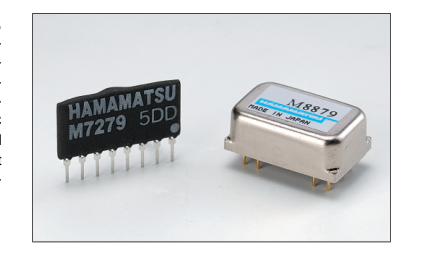
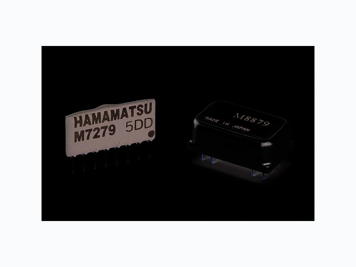
The M7279 and M8879 are non-inverting amplifier modules, specifically designed for photodetectors such as photomultiplier tubes. These amplifier modules work with either a current or voltage input, allowing direct connection to a photomultiplier tube or other photodetectors. The M7279 is comprised of an 8-pin SIP (single inline package) type hybrid IC with protective epoxy resin and the M8879 is a 10-pin hybrid IC to allow a compact mounting size on PC board. The offset voltage and gain are easily adjusted by connecting an external variable resistor.
FEATURES
G Non-inverting Amplifier Modules
G Compact Size G Current-to-Voltage Conversion Factor
G Frequency Bandwidth
M7279: 10 mV/µA
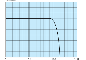
M7279: DC to 10 MHz
M8879: 4 mV/µA
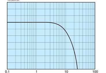
M8879: DC to 150 MHz
SPECIFICATIONS
MAXIMUM RATINGS (Absolute Maximum Values)
| Parameter | M7279 | M8879 | Unit |
|---|---|---|---|
| Power Supply Voltage (±Vs) | ±7 | ±6.5 | V |
| Operating Temperature Range | -20 to +55 | 0 to +40 | °C |
| Storage Temperature Range | -30 to +85 | -15 to +60 | °C |
| Signal Input Voltage | ±Vs | V | |
| Lead Soldering Temperature (Less than 5 s) | +280 | °C | |
CHARACTERISTlCS (at 25 °C, ±Vs = ±5 V)
| Parameter | M7279 | M8879 | Unit | ||
|---|---|---|---|---|---|
| Voltage Gain | Load Resistance: 50 Ω | 100 | 80 | — | |
| Frequency Bandwidth (-3 dB) | See Figure 1, 2 | DC to 10 | DC to 150 | MHz | |
| Current-to-Voltage Conversion Factor | Load Resistance: 50 Ω | 10 | 4 | mV/µA | |
| Input Polarity | Positive / Negative | — | |||
| Amplifying Method | Non-inverting Output | — | |||
| Input Impedance | 100 | 50 | Ω | ||
| Output Impedance | 50 | Ω | |||
| Maximum Output Voltage | Load Resistance: 50 Ω | Min. | ±1.5 | ±1.4 | V |
| Load Resistance: 1 MΩ | Min. | ±3.5 | ±3 | V | |
| Output Noise Voltage | Load Resistance: 50 Ω | Typ. | 1.0 | 2.8 | mVrms |
| Temperature Coefficient of Output Offset Voltage | Operating Temperature Range Load Resistance: 50 Ω | ±0.3 | ±0.2 | mV/°C | |
| Power Supply Voltage | Recommended Supply Voltage | ±5 to ±6.5 | ±5 to ±6 | V | |
| Power Supply Current | Max. | 45 | 61 | mA | |
| Weight | 1.1 | 2.5 | g | ||
Subject to local technical requirements and regulations, availability of products included in this promotional material may vary. Please consult with our sales office. Information furnished by HAMAMATSU is believed to be reliable. However, no responsibility is assumed for possible inaccuracies or omissions. Specifications are subject to change without notice. No patent rights are granted to any of the circuits described herein. ©2010 Hamamatsu Photonics K.K.
Page 2
AMPLIFIER MODULES M7279, M8879
GTypical Frequency Response
Figure 1: M7279
Figure 2: M8879
TACCB0057EA
TACCB0063EB
FREQUENCY (MHz)
FREQUENCY (MHz)
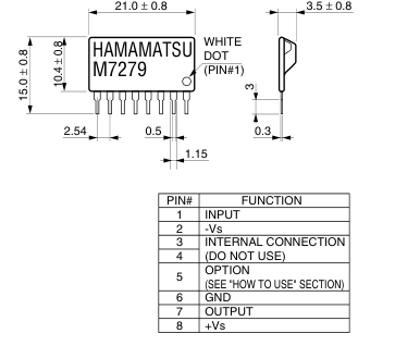
GDimensional Outline and Pin Configuration (Unit: mm)
Figure 3: M7279
Figure 4: M8879
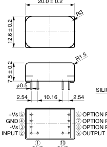
METAL CASE
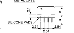
OPTION PIN A OPTION PIN B (SEE "HOW TO USE" SECTION) OPTION PIN C
GND GND
TACCA0183ED
TACCA0249EA
White dot mark is located on the character printed side to show the orientation of pin#1.
Page 3
HOW TO USE
GM7279
(A)
(B)
To adjust the offset voltage: The DC offset voltage level varies with the ambient temperature and the internal impedance of the signal lines. To adjust this offset voltage level, externally connect a variable resistor across the option lead pins as shown in figure (A) on the right. If a capacitor is connected to pin 7 as shown in figure (B) on the right, this acts as AC
COUPLING
coupling and eliminates the offset voltage.
200 kΩ
CAPACITOR OUTPUT
To adjust the gain: To adjust the gain of the M7279, externally connect a resistor (Re) across pins 5 and
VR (10 kΩ to 20 kΩ)
6 as shown in the figure below. Use a resistor of 150 Ω or more. The M7279 can be
-Vs
+Vs
TACCC0109EA
used at a gain between (1) and (2) shown in the gain graph.
Variation of gain and frequency response
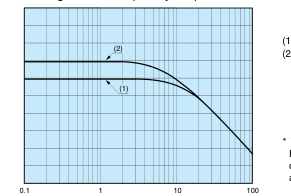
GAIN INCREASING
WITHOUT RESISTOR 150 Ω RESISTOR BETWEEN PINS #5 AND #6
Re 150 Ω >=
\* The output offset voltage also changes when Re is connected to the M7279. Adjust the offsett voltage by referring to the offsett voltage adjustment method explained above.
FREQUENCY (MHz)
TACCB0058EA
PC board layout When designing the PC board layout for mounting the M7279, the input signal line (pin 1) must be kept as short as possible to avoid impairing the high-speed response. Do not connect the supply voltage (±Vs) to pins 1, 3, 4, 5 and 7. Use a wide area for ground. Connect external bypass capacitors between the power supply lines (±Vs) and ground, and keep the wiring as short as possible. The output impedance of the M7279 is 50 Ω. Make sure the signal output line matches the 50 Ω impedance. When mounting the M7279 on a PC board, directly insert the pins into the terminal holes on the PC board without using any socket. We recommend connecting diodes to pin 1 as shown below for over-current protection.
Don't connect any of option pins to anywhere in circuit unless using the option. Keep on disconnecting condition when not used.
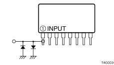
TACCC0111EA
Page 4
AMPLIFIER MODULES M7279, M8879
HOW TO USE
GM8879
(A)
(B)
To adjust the offset voltage: The DC offset voltage level varies with the ambient temperature and the internal impedance of the signal lines. To adjust this offset voltage level, externally connect a variable resistor across the op- tion lead pins as shown in figure (A) on the right. If a capacitor is connected to pin 9 as shown in figure (B) on the right, this acts as AC coupling and
6 7 8
eliminates the offset voltage.
9
COUPLING
PC board layout
CAPACITOR
When designing a PC board layout for mounting the M8879, it is recommended to follow below
OUTPUT
OFFSET VR
suggestion in order to maintain its high-speed response.
10 kΩ
- The pattern for input signal line and output signal line should not be longer than 7 mm and con-
(TOP VIEW)
nection should be made with coaxial cable.
TACCC0118EA
(The characteristic impedance of coaxial cable should be 50 Ω and the length of core cable should be as short as possible.) Use a cable clamp or a cable crimp type connector to a coaxial (cable).
- All of pins from the M8879 should be connected on a PC Board.
- Do not connect the supply voltage (±Vs) to the pins 2, 6, 7, 8 and 9.
- Use a wide area for ground.
- Connect external bypass capacitors between the power supply lines (±Vs) and ground, and keep the wiring as short as possible.
- The output impedance of the M8879 is 50 Ω. Make sure the signal output line matches 50 Ω im- pedance.
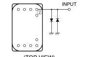
- When mounting the M8879 on a PC board, directly insert the pins into the terminal holes on the PC board without using any socket. We recommend connecting diodes to pin 2 as shown on the
(TOP VIEW)
right for over-current protection.
TACCC0119EA
- Don't connect any of option pins to anywhere in circuit unless using the option. Keep on discon- necting condition when not used.

WEB SITE www.hamamatsu.com
HAMAMATSU PHOTONICS K.K., Electron Tube Division 314-5, Shimokanzo, Iwata City, Shizuoka Pref., 438-0193, Japan, Telephone: (81)539/62-5248, Fax: (81)539/62-2205 U.S.A.: Hamamatsu Corporation: 360 Foothill Road, P. O. Box 6910, Bridgewater. N.J. 08807-0910, U.S.A., Telephone: (1)908-231-0960, Fax: (1)908-231-1218 E-mail: usa@hamamatsu.com Germany: Hamamatsu Photonics Deutschland GmbH: Arzbergerstr. 10, D-82211 Herrsching am Ammersee, Germany, Telephone: (49)8152-375-0, Fax: (49)8152-2658 E-mail: info@hamamatsu.de France: Hamamatsu Photonics France S.A.R.L.: 19, Rue du Saule Trapu, Parc du Moulin de Massy, 91882 Massy Cedex, France, Telephone: (33)1 69 53 71 00, Fax: (33)1 69 53 71 10 E-mail: infos@hamamatsu.fr
United Kingdom: Hamamatsu Photonics UK Limited: 2 Howard Court, 10 Tewin Road Welwyn Garden City Hertfordshire AL7 1BW, United Kingdom, Telephone: 44-(0)1707-294888, Fax: 44(0)1707-325777 E-mail: info@hamamatsu.co.uk North Europe: Hamamatsu Photonics Norden AB: Smidesvägen 12, SE-171-41 SOLNA, Sweden, Telephone: (46)8-509-031-00, Fax: (46)8-509-031-01 E-mail: info@hamamatsu.se Italy: Hamamatsu Photonics Italia: S.R.L.: Strada della Moia, 1/E, 20020 Arese, (Milano), Italy, Telephone: (39)02-935 81 733, Fax: (39)02-935 81 741 E-mail: info@hamamatsu.it
TACC1044E01 MAR. 2010. IP