
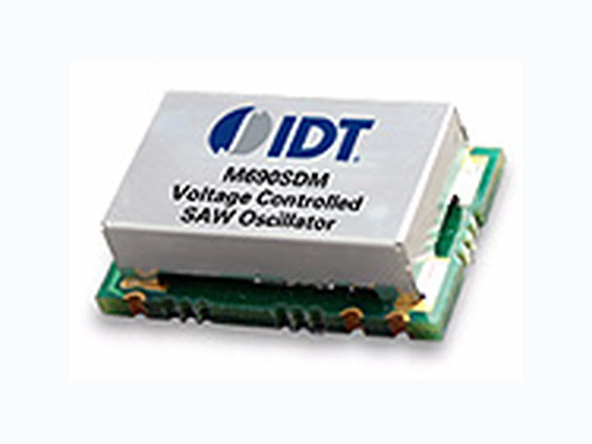
M690SDM RENESAS
Document overview
- Manufacturer or author: atassone
- PDF pages: 6
Technical content
SIGE SINGLE FREQUENCY VCSO Performance Datasheet GENERAL DESCRIPTION The M690SDM is a single frequency/single output SAW-based VCSO for low-jitter clock generation. The M690SDM incorporates an analog X2 frequency multiplier to provide an output frequency that is twice that of the fundamental VCSO frequency.
FEATURES
◆ Integrated SAW device ◆ Low phase jitter: 250fs rms typical for the M690SDM (20kHz to 20MHz) ◆ Output frequency: 1747 MHz Typ. (Specify center frequency at time of order) ◆ Single-ended RF Output ◆ Single +5V power supply ◆ 13 x 20mm SMT (surface mount) package ◆ Pb-free / Compliant to EC RoHS Directive (RoHS 5/6) PIN ASSIGNMENT (13 x 20mm SMT) Figure 1: Pin Assignment BLOCK DIAGRAM Figure 2: Block Diagram Sample of Available Output Frequencies VCSO Center Frequencies1 (MHz) Note 1: Specify VCSO center frequency at time of order. Other frequencies available upon request. Output Frequency Code
1747.623000 R01
1747.030837 R02
1748.366885 R03
1748.793733 R04
Table 1: Sample of Available Output Frequencies SAW Delay Line M690SDM SiGe Single Frequency VCSO
SIGE SINGLE FREQUENCY VCSO Performance Datasheet PIN DESCRIPTIONS Number Name I/O Configuration Description 1V I N Input Frequency control input. 2, 3, 5 GND Ground Power supply ground connection. 4 RF OUTPUT Output No internal terminator Clock output. Single-ended. 6V C C Power Power supply connection, connect to +5.0 V. Table 2: Pin Descriptions ABSOLUTE MAXIMUM RATINGS1 Note 1: Stresses beyond those listed under Absolute Maximum Ratings may cause permanent damage to the device. These ratings are stress specifications only. Functional operation of product at these conditions or any conditions beyond those listed in Recommended Conditions of Operation, DC Characteristics, or AC Characteristics is not implied. Exposure to absolute maximum rating conditions for extended periods may affect product reliability. Symbol Parameter Rating Unit VI Inputs -0.5 to VCC +0.5 V VO Outputs -0.5 to VCC +0.5 V VCC Power Supply Voltage 6.0 V TS Storage Temperature -55 to +125 oC Table 3: Absolute Maximum Ratings RECOMMENDED CONDITIONS OF OPERATION Symbol Parameter Min Typ Max Unit VCC Positive Supply Voltage 4.875 5.0 5.125 V TCASE Operating Temperature +10 +85 oC Table 4: Recommended Conditions of Operation
ww w.idt.com ● tel (774) 348-1600 M690SDM SIGE SINGLE FREQUENCY VCSO Performance Datasheet ELECTRICAL SPECIFICATIONS DC Characteristics for M690SDM Unless stated otherwise, VCC = 5.0 Volts + 2.5%, TCASE = 10 to 85 oC, VCSO Frequency = 1747.623000, Output terminated with 50Ω. Symbol Parameter Pin Min Typ Max Unit Power Supply VCC Positive Supply Voltage VCC 4.875 5.0 5.125 V ICC Power Supply Current 145 165 mA Control Voltage VIN Input Control Voltage Range VIN 0 3.3 V VIN Input Impedence 20 kΩ Table 5: DC Characteristics for M690SDM AC Characteristics for M690SDM Unless stated otherwise, VCC = 5.0 Volts + 2.5%, TCASE = 10 to 85 oC, VCSO Frequency = 1747.623000, Outputs terminated with 50Ω. Symbol Parameter Min Typ Max Unit Notes Control Voltage VIN Modulation Bandwidth VIN 500 kHz Output RF OUTPUT Output Center Frequency Range 1500 2100 MHz POUTPUT Output Power 7.5 10.0 12.0 dBm 50Ω load; AC Coupled TRANGE Tuning Range 1000 ppm Note 1: Also fully meets ±50 ppm minimum pull-range. ±100 ppm fSTAB Frequency Stability 300 ppm p-p 10ºC to 85ºC Power Supply Pushing -32 32 ppm VCC = 5.0V±2.5V LIN Tuning Linearity -8 8 % Deviation from best Linear fit KVCO VCO Gain @1747.623000MHz 340 ppm/V Harmonic Spurious -30 dBc Sub-harmonic Spurious -30 dBc Non-harmonic Spurious -60 dBc VSWR Load VSWR, all phases 3.5:1 Φ n SS B (single sideband) Phase Noise, offset from carrier @1747.623000MHz 10kHz Offset -95 dBc/Hz 100kHz Offset -116 dBc/Hz 1MHz Offset -134 dBc/Hz 10MHz Offset -140 dBc/Hz 20MHz Offset -143 dBc/Hz Table 6: AC Characteristics for M690SDM
SIGE SINGLE FREQUENCY VCSO Performance Datasheet DEVICE PACKAGE - 13 x 20mm SMT (Surface Mount) Package Mechanical Dimensions: Figure 3: Device Package - 13 x 20mm SMT (Surface Mount Package) M690 PIN OUT PIN 1 VIN PIN 2 GND PIN 3 GND PIN 4 RF OUTPUT PIN 5 GND PIN 6 VCC 13.0 [0.512] 2.4 [0.094] 15.2 [0.600] 2.5 [0.100] 1.6 [0.062] T O P VIEW 6 5 4 1 2 3 6x 1.9 [0.073] 6x 1.2 [0.049]
6.35 MAX
0.250 MAX
Pad Finish: Gold over Nickel MSL 1
SIGE SINGLE FREQUENCY VCSO Performance Datasheet
ORDERING INFORMATION
Figure 4: Part Numbering Scheme Example Order Numbers M690SDM Standard Output Frequencies & Order Codes Consult IDT for the availability of other frequencies For Output Frequencies (MHz) Frequency Order Part Number M690SDM-xxx
1747.623000 M690SDM-R01
1747.030837 M690SDM-R02
Table 7: Example Order Numbers M690SD Part Number: M680-01 - See Table 8 at right for frequency order codes. Device Number Consult IDT for other frequencies and order codes. M690SDM Output Frequency Order Code xxx Output Frequency Code Output Frequency MHz R01 1747.623000 R02 1747.030837 R03 1748.366885 R04 1748.793733 Table 8: M690SDM Standard Output Frequencies & Order
© 202 Renesas Electronics Corporation. All rights reserved. IMPORTANT NOTICE AND DISCLAIMER RENESAS ELECTRONICS CORPORATION AND ITS SUBSIDIARIES (“RENESAS”) PROVIDES TECHNICAL SPECIFICATIONS AND RELIABILITY DATA (INCLUDING DATASHEETS), DESIGN RESOURCES (INCLUDING REFERENCE DESIGNS), APPLICATION OR OTHER DESIGN ADVICE, WEB TOOLS, SAFETY INFORMATION, AND OTHER RESOURCES “AS IS” AND WITH ALL FAULTS, AND DISCLAIMS ALL WARRANTIES, EXPRESS OR IMPLIED, INCLUDING, WITHOUT LIMITATION, ANY IMPLIED WARRANTIES OF MERCHANTABILITY, FITNESS FOR A PARTICULAR PURPOSE, OR NON-INFRINGEMENT OF THIRD PARTY INTELLECTUAL PROPERTY RIGHTS. These resources are intended for developers skilled in the art designing with Renesas products. You are solely responsible for (1) selecting the appropriate products for your application, (2) designing, validating, and testing your application, and (3) ensuring your application meets applicable standards, and any other safety, security, or other requirements. These resources are subject to change without notice. Renesas grants you permission to use these resources only for development of an application that uses Renesas products. Other reproduction or use of these resources is strictly prohibited. No license is granted to any other Renesas intellectual property or to any third party intellectual property. Renesas disclaims responsibility for, and you will fully indemnify Renesas and its representatives against, any claims, damages, costs, losses, or liabilities arising out of your use of these resources. Renesas' products are provided only subject to Renesas' Terms and Conditions of Sale or other applicable terms agreed to in writing. No use o any Renesas resources expands or otherwise alters any applicable warranties or warranty disclaimers for these products. ('LVFODLPHURev.1.0 Mar 2020) Corporate Headquarters Contact Information TOYOSU FORESIA, 3-2-24 Toyosu, For further information on a product, technology, the most Koto-ku, Tokyo 135-0061, Japan up-to-date version of a document, or your nearest sales www.renesas.com office, please visit: www.renesas.com/contact/ Trademarks Renesas and the Renesas logo are trademarks of Renesas Electronics Corporation. All trademarks and registered trademarks are the property of their respective owners.