
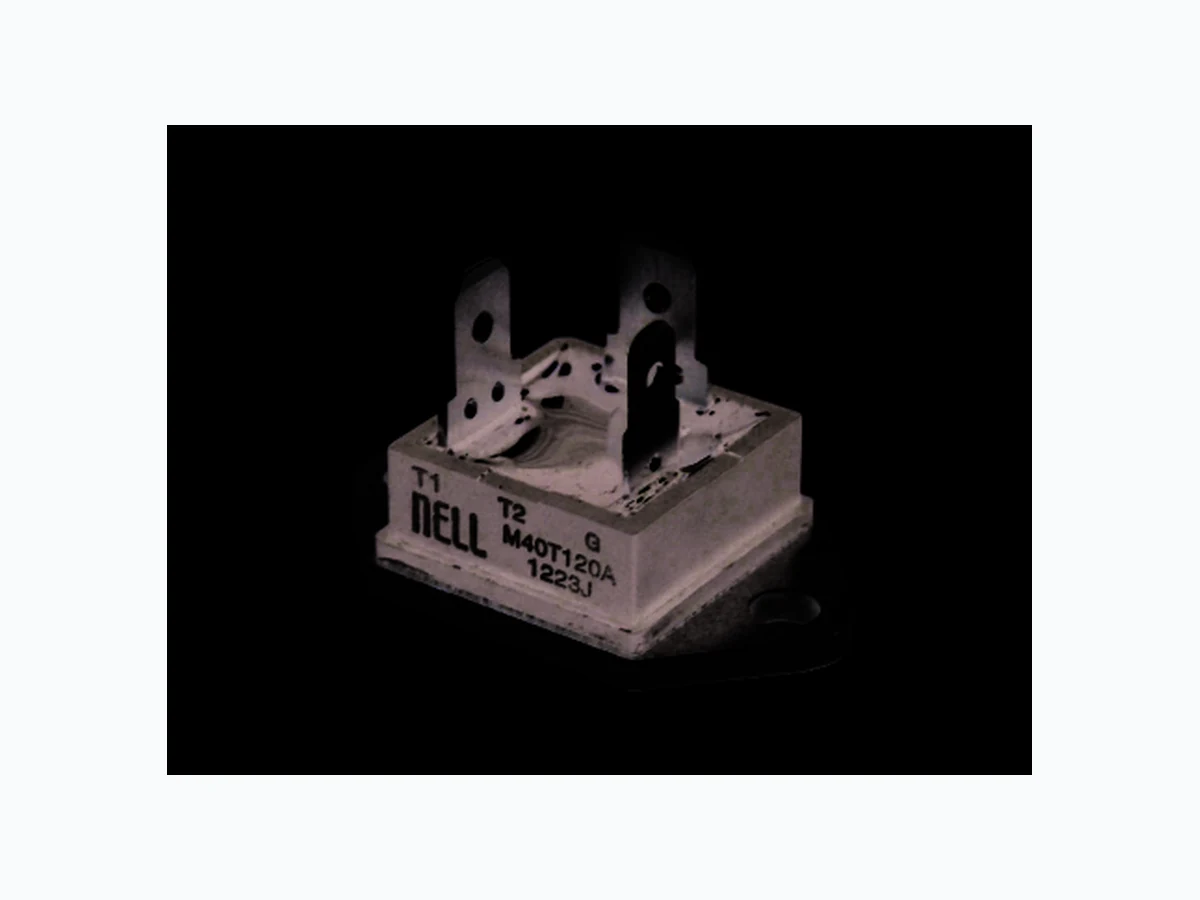
M40T NELLSEMI
Document overview
- Manufacturer or author: Provided By www.digicamel.com(FREE DATASHEET DOWNLOAD SITE)
- PDF pages: 5
Technical content
www.nellsemi.com Page 1 of 5 SEMICONDUCTOR M40T Series RoHS RoHS TRIACs, 40A
FEATURES
APPLICATIONS
Low thermal resistance with clip bonding Low thermal resistance insulation ceramic for insulated TO-3 package High commutation capability MAIN FEATURES SYMBOL VALUE UNIT IT(RMS) V /VDRM RRM IGT(Q1) 40 A V mA10 to 50 600 to 1200 Sunbberless Packages are RoHS compliant SYMBOL IT(RMS)RMS on-state current (full sine wave) ITSM Non repetitive surge peak on-state current (full cycle, T initial = 25°C)j A I t22I t Value for fusing 800 2A s dI/dt Critical rate of rise of on-state current I = 2xl , t ≤100nsG GT r IGMPeak gate current 4 PG(AV)Average gate power dissipation 1 PGM 10 W A/µs A A UNITVALUE 400 420 F =50 Hz F =60 Hz t = 20 ms t = 16.7 ms t = 10 msp F =100 Hz T =125ºCj T =125ºCj T =125ºCj T =20 µsp ABSOLUTE MAXIMUM RATINGS PARAMETER TEST CONDITIONS T = 90ºCc 40 TstgStorage temperature range Operating junction temperature range - 40 to + 150 - 40 to + 125 ºC Tj Peak gate power dissipation (tp = 20µs) T =125ºCj T1 T2 G Due to their clip assembly techinque, they provide a superior performance in surge current handling capabilities. By using an internal ceramic pad, the M40T series provides voltage insulated tab (rated at 2500VRMS) complying with UL standards. The snubberless concept offer suppression of RC network and it is suitable for applications such as : Static relays Solid state switches Motor controls Copy machines Microwave ovens Heater controls Light dimmers
www.nellsemi.com Page 2 of 5 SEMICONDUCTOR RoHS RoHS V (2)TM MAX. Vt0(2) Threshold voltage MAX. Dynamic resistance MAX. IDRM IRRM MAX. mA Note 1: Minimum l is guaranted at 5% of l max.GT GT Note 2: For both polarities of A2 referenced to A1. I = 60 A, TM t = 380 µsP T = 125°Cj T = 25°Cj T = 125°Cj T = 125°Cj T = 25°Cj 1.55 0.85 V V µA mΩ STATIC CHARACTERISTICS UNITVALUETEST CONDITIONS SYMBOL (2)Rd V = VD DRM V = VR RRM Limits Unit I (1)GT I - II - III VGT I - II - III VGD I - II - III (2)IH MAX. I - III MAX. mA II (2)dV/dt MIN. (dI/dt)c (2) A/ms IL MAX. MIN. V = 12 V, R = 33ΩD L V = V , R = 3.3KΩD DRM L T = 125°Cj I = 500 mAT I = 1.2 IG GT V = 67% V gate open ,T = 125°CD DRM j, Without snubber, T = 125°Cj 1.3 0.2 150 1000 mA V V mA V/µs TEST CONDITIONS QUADRANTSYMBOL BW SNUBBERLESS and Logic level (3 quadrants) (T ºC unless otherwise specified)J= 25 ELECTRICAL CHARACTERISTICS THERMAL RESISTANCE Rth(j-c) Junction to case (AC) Rth(j-a) Junction to ambient 0.8 °C/W UNITVALUESYMBOL S = Copper surface under tab.
ORDERING INFORMATION
ORDERING TYPE MARKING PACKAGE WEIGHT ,BASE Q TY DELIVERY MODE TO-3 23g 50 BOX PRODUCT SELECTOR PART NUMBER VOLTAGE (xx) SENSITIVITY PACKAGE 800 V 50 mAM40TxxA TYPE V 1000 V V Snubberless TO-3 1200 V V 600 V V M40T Series M40TxxA Note : xx = voltage
www.nellsemi.com Page 3 of 5 ORDERING INFORMATION SCHEME Triac series Current Voltage 40 = 40A 60 = 600V 80 = 800V Assembly type 100 = 1000V A = Soldering Assembly
40 T 60 A
Fig.1 Maximum power dissipation versus on-state RMS current (full cycle) Fig.2 On-state RMS current versus case temperature (full cycle) P (W) I (A)T(RMS) 125100755025 Fig.3 Relative variation of thermal impedance versus pulse duration. Fig.4 On-state characteristics (maximum values). 1E-03 1E-02 1E-01 1E+00 K=[Z /R ]th th 1E+0.31E+021E+011E+001E-011E-02 0 5 10 15 20 25 1E-03 I (A)T(RMS) 30 35 40 180° α α α=180° Zth(j-c) tp(s) T max.j V = 0.85 Vto R = 10 mΩd T =T maxj j T =25°Cj V (V)TM 100 400 I (A)TM 120 = 1200V M40T Series M Module type M = TO-3 Fast-on package Tc(°c)
www.nellsemi.com Page 4 of 5 0.01 2 2I (A),l t(A s)TSM 1.000.10 Fig.7 Relative variation of gate trigger, holding and latching current versus junction temperature. Fig.9 Relative variation of critical rate of decrease of main current versus (dV/dt)c. 100 150 200 250 1 10 100 1000 300 100 1000 10000 Fig.5 Surge peak on-state current versus number of cycles. 350 400 450 t=20ms One cycle Non repetitive T initial=25°Cj Repetitive T =70°Cc Number of cycles Fig.6 Non-repetitive surge peak on-state current for a sinusoidal pulse and corresponding 2 value of l t. t (ms)p 2I t ITSM dl/dt limitation 50A/µs T initial =25°Cj Pulse width tp <10 ms 10.00 l ,l ,l [T ] / l ,l ,l [T =25°C]GT H L j GT H L j 0.0 0.5 1.0 1.5 2.0 2.5 -40 -20 0 20 40 60 80 100 120 140 T (°C)j Fig.8 Relative variation of critical rate of decrease of main current versus (dV/dt)c (typical values). 0.4 0.8 1.2 1.6 2.0 (dI/dt)c [(dV/dt)c] / specified (dI/dt)c 0.1 1.0 10.0 100.0 1.8 1.4 1.0 0.6 (dV/dt)c (V/µs) (dI/dt)c [T ] / j (dI/dt)c [T specified]j 0 25 50 75 100 125 T (°C)j I (A)TSM l & lH L lGT Typical values M40T Series
0.35±0.15 2-Ø4.2±0.1 30.0±0.1 Ø1.3(G) 9.75±0.3 www.nellsemi.com Page 5 of 5 All dimensions in millimeters TO-3 Case Style