
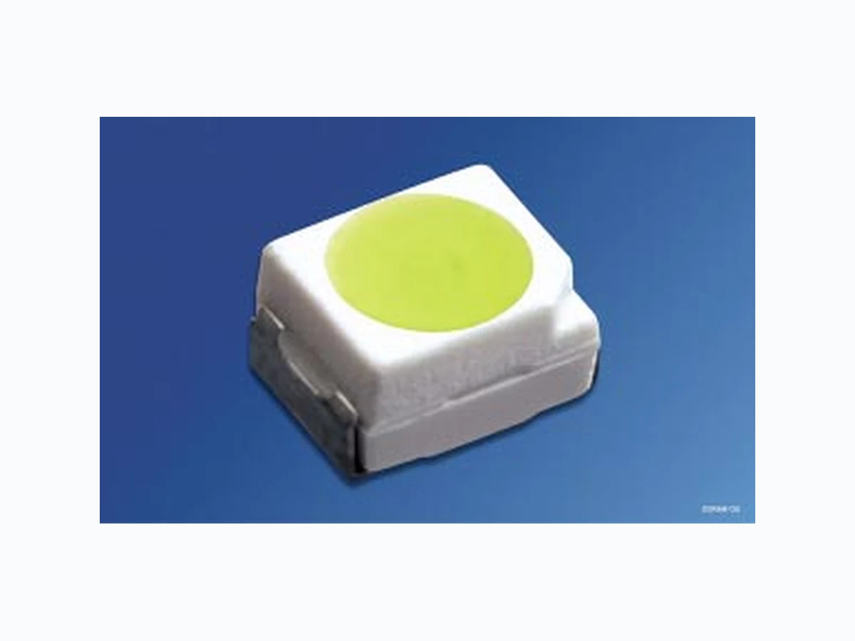
LWT673 OSRAM
Document overview
- Manufacturer or author: Provided By www.digicamel.com(FREE DATASHEET DOWNLOAD SITE)
- PDF pages: 14
Technical content
Features
- package: white P-LCC-2 package
- feature of the deivce: extremely wide viewing angle; ideal for backlighting and coupling in light guides
- color coordinates:x = 0.32, y = 0.31 acc. to CIE 1931 (white)
- typ. color temperature:6500 K
- color reproduction index:85
- viewing angle:Lambertian Emitter (120°)
- technology:InGaN
- optical efficiency:6l m / W
- grouping parameter:luminous intensity, color coordinates
- assembly methods: suitable for all SMT assembly methods
- soldering methods:IR reflow soldering and TTW soldering
- preconditioning:acc. to JEDEC Level 2
- taping:8 mm tape with 2000/reel, ø180 mm or 8000/reel, ø330 mm
- ESD-withstand voltage:up to 2 kV acc. to MIL STD 883 D, Method 3015.7
Applications
- outdoor displays
- backlighting (LCD, switches, keys, displays, illuminated advertising)
- interior and exterior automotive lighting
- substitution of micro incandescent lamps, reading lamps
- emergency lighting
- signal and symbol luminaire
- marker lights (e.g. steps, exit ways, etc.)
- scanners
Helligkeitswerte werden mit einer Stromeinprägedauer von 25 ms und einer Genauigkeit von ±11 % ermittelt. Luminous intensity is tested at a current pulse duration of 25 ms and an accuracy of ±11 %. -1 Farbselektiert nach Farbortgruppen (siehe Seite 5). -1 Color selection acc. to Chromaticity coordinate groups (see page 5). Typ Type Emissions- farbe Color of Emission Farbe der Lichtaustritts- fläche Color of the Light Emitting Area Lichtstärke Luminous Intensity IF =2 0m A IV (mcd) Lichtstrom Luminous Flux IF =2 0m A /G46 V (mlm) Bestellnummer Ordering Code LW T673-Q2R2-1 LW T673-R2S2-1 LW T673-Q2 LW T673-R1 LW T673-R2 LW T673-S1 LW T673-S2 white colored diffused 90 ... 180 140 ... 280 90 ... 112 112 ... 140 140 ... 180 180 ... 224 224 ... 280 405 (typ.) 630 (typ.) 303 (typ.) 378 (typ.) 480 (typ.) 606 (typ.) 756 (typ.) Q62703-Q4836 Q62703-Q4686
Operating temperature range Top – 40 … + 100 °C Lagertemperatur Storage temperature range Tstg – 40 … + 100 °C Sperrschichttemperatur Junction temperature Tj + 110 °C Durchlassstrom Forward current IF 20 mA Stoßstrom Surge current t/Ga3/G20 10 /G6d s,D = 0.005 IFM 200 mA Sperrspannung Reverse voltage VR 5V Leistungsaufnahme Power dissipation TA /Ga3 25 °C Ptot 85 mW Wärmewiderstand Thermal resistance Sperrschicht/Umgebung Junction/ambient Sperrschicht/Lötpad Junction/solder point Montage auf PC-Board FR 4 (Padgröße /Gb3 16 mm 2) mounted on PC board FR 4 (pad size/Gb3 16 mm 2) Rth JA Rth JS 400 180 K/W K/W
Kennwerte (TA =2 5° C ) Characteristics Bezeichnung Parameter Symbol Symbol Wert Value Einheit Unit Farbkoordinate x nach CIE 19311) (typ.) Chromaticity coordinate x acc. to CIE 19311) IF =2 0m A x0 . 3 2– Farbkoordinate y nach CIE 19311) (typ.) Chromaticity coordinate y acc. to CIE 19311) IF =2 0m A y0 . 3 1– Abstrahlwinkel bei 50 %IV (Vollwinkel) (typ.) Viewing angle at 50 %IV 2/G6a 120 Grad deg. Durchlassspannung (typ.) Forward voltage (max.) IF =2 0m A VF VF 3.5 4.2 V V Sperrstrom (typ.) Reverse current (max.) V R =5V IR IR 0.01 /G6d A /G6d A Temperaturkoeffizient von x (typ.) Temperature coefficient of x IF =2 0m A ;– 1 0 ° C/Ga3/G20 T /Ga3/G20 100°C TC x 0.1 10 -3/K Temperaturkoeffizient von y (typ.) Temperature coefficient of y IF =2 0m A ;– 1 0 ° C/Ga3/G20 T /Ga3/G20 100°C TC y 0.3 10 -3/K Temperaturkoeffizient vonV F (typ.) Temperature coefficient ofVF IF =2 0m A ;– 1 0 ° C/Ga3/G20 T /Ga3/G20 100°C TC V –3 . 0 m V / K Optischer Wirkungsgrad (typ.) Optical efficiency IF =2 0m A /G68 opt 6l m / W
1) Farbortgruppen Chromaticity coordinate groups Gruppenbezeichnung auf Etikett Group Name on Label Beispiel: R2-4 Example: R2-4 Farbortgruppen werden mit einer Stromeinprägedauer von 25 ms und einer Genauigkeit von ±0,01 ermittelt. Chromaticity coordinate groups are tested at a current pulse duration of 25 ms and an accuracy of ±0.01. Lichtgruppe Luminous Intensity Group Halbgruppe Half Group Farbortgruppe Cromaticity coordinate Group R2 4 OHA01327 520 530 540 550 560 570 580 590 600 610 620 630 0.1 0.2 0.3 0.4 0.5 0.6 0.7 0.8 0.9 510 500 490 480 470 450 460 0.28 0.23 0.24 0.30 0.32 0.34 0.36 0.25 0.26 0.27 0.28 0.29 0.30 0.31 0.32 0.33 0.34 0.35 0.36 0.37 0.38 0.39 0.40 0.38 group 3 group 4 group 5 E 0.29 0.31 0.33 0.35 Cx
Relative spektrale EmissionIrel= f(/G6c ),TA =2 5° C ,IF =2 0m A Relative Spectral Emission /G6c ) = spektrale Augenempfindlichkeit Standard eye response curve AbstrahlcharakteristikIrel= f(/G6a ) Radiation Characteristic OHL00609 400 100 Irel λ nm450 500 550 600 650 700 λV 0.2 0.4 1.0 0.8 0.6 ϕ 1.0 0.8 0.6 0.4 50˚ 60˚ 70˚ 80˚ 90˚ 100˚
Durchlassstrom IF = f(VF) Forward Current TA =2 5° C Maximal zulässiger DurchlassstromIF = f(T) Max. Permissible Forward Current Relative LichtstärkeIV/IV(20 mA) = f(IF) Relative Luminous Intensity TA =2 5° C Maximal zulässiger DurchlassstromIF = f(T) Max. Permissible Forward Current OHL00611 10 -1 2.5 3 3.5 4 4.5 V 5 010 110 10 2 mA IF VF OHL00867 0 0 ˚C mA 20 40 60 80 100 IF 5000 h 10000 h T temp. ambientTA MTTF MTTF V V (20 mA) 10 -1 0 10 10 12 10mA 10 -3 OHL00623 I I 10 -2 10 -1 10 0 10 1 FI OHL01086 00 20 40 60 80 ˚C 100 T IF mA temp. solder pointST 10000 h 5000 hMTTF MTTF
Relative LichtstärkeIV/IV(25 °C)= f(TA ) Relative Luminous Intensity IF =2 0m A Zulässige ImpulsbelastbarkeitIF = f(tp) Permissible Pulse Handling Capability Duty cycle D = parameter,TA =2 5° C Farbortverschiebungx, y =f(IF) Chromaticity Coordinate Shift TA =2 5° C Zulässige ImpulsbelastbarkeitIF = f(tp) Permissible Pulse Handling Capability Duty cycle D = parameter,TA=8 5° C OHL00870 0-10 V V (25 ˚C)I I V AT 10 30 50 70 100 0.2 0.4 0.6 0.8 1.2 OHL01405 FI 10 10-5 -4 -3 10 10 -2 10-1 100 s101 102 pt 0.05 0.10 0.15 0.20 0.25 0.30 0.05 0.5 0.2 0.1 D 0.02 0.01 0.005 A D T t = P t T P IF OHL00655 0.30401 0 2 0 30 x, y 50mA 0.306 0.308 0.310 0.312 0.314 0.316 0.318 0.324 x y FI OHL01406 FI 10 10-5 -4 -3 10 10 -2 10-1 100 s101 102 pt 0.05 0.10 0.15 0.20 0.25 0.30 0.05 0.5 0.2 0.1 D 0.02 0.01 0.005 A D T t = P t T P IF
Maßzeichnung Package Outlines Maße werden wie folgt angegeben: mm (inch) / Dimensions are specified as follows: mm (inch). Kathodenkennung: abgeschrägte Ecke Cathode mark: bevelled edge GPLY6724 0.7 (0.028) 0.9 (0.035) 1.7 (0.067) 2.1 (0.083) 0.12 (0.005) 0.18 (0.007) 0.5 (0.020) 3.7 (0.146) 0.4 (0.016) 0.6 (0.024) 2.6 (0.102) 3.0 (0.118) 2.1 (0.083) 2.3 (0.091) Cathode marking 3.0 (0.118) 3.4 (0.134) (2.4) (0.095) 0.1 (0.004) (typ.) 4˚±1
Lötbedingungen Vorbehandlung nach JEDEC Level 2 Soldering ConditionsPreconditioning acc. to JEDEC Level 2 IR-Reflow Lötprofil (nach IPC 9501) IR Reflow Soldering Profile(acc. to IPC 9501) OHLY0597 50 100 150 200 250 100 150 200 250 300 T t s 240-245 ˚C 10-40 s 183 ˚C 120 to 180 s Defined for Preconditioning: up to 6 K/s Ramp-down rate up to 6 K/s Ramp-up rate up to 6 K/s Defined for Preconditioning: 2-3 K/s
Wellenlöten (TTW) (nach CECC 00802) TTW Soldering (acc. to CECC 00802) OHLY0598 50 100 150 200 250 100 150 200 250 300 T t C s 235 C 10 s C... 260 1. Welle 1. wave 2. Welle 2. wave
5 K/s 2 K/sca 200 K/s
CC... 130100
2 K/s
Zwangskühlung forced cooling Normalkurve standard curve Grenzkurven limit curves
Empfohlenes Lötpaddesign IR Reflow Löten / Wellenlöten (TTW) Recommended Solder Pad IR Reflow Soldering / TTW Soldering Maße werden wie folgt angegeben: mm (inch) / Dimensions are specified as follows: mm (inch). OHLPY970 4.5 (0.177) 2.6 (0.102) 1.5 (0.059) Paddesign for improved heat dissipation Cu-area > 16 mm Cu-Fläche > 16 mm für verbesserte Padgeometrie Wärmeableitung Solder resist Lötstopplack 4.5 (0.177) 1.5 (0.059) 2.6 (0.102)
Gurtung / Polarität und Lage Verpackungseinheit 2000/Rolle, ø180 mm oder 8000/Rolle, ø330 mm Method of Taping / Polarity and OrientationPacking unit 2000/reel, ø180 mm or 8000/reel, ø330 mm Maße werden wie folgt angegeben: mm (inch) / Dimensions are specified as follows: mm (inch). OHAY2271 C A 3.6 (0.142) 8 (0.315) 3.5 (0.138) 1.75 (0.069) 2 (0.079)
Published by OSRAM Opto Semiconductors GmbH & Co. OHG Wernerwerkstrasse 2, D-93049 Regensburg © All Rights Reserved. Attention please! The information describes the type of component and shall not be considered as assured characteristics. Terms of delivery and rights to change design reserved. Due to technical requirements components may contain dangerous substances. For information on the types in question please contact our Sales Organization. Packing Please use the recycling operators known to you. We can also help you – get in touch with your nearest sales office. By agreement we will take packing material back, if it is sorted. You must bear the costs of transport. For packing material that is returned to us unsorted or which we are not obliged to accept, we shall have to invoice you for any costs incurred. Components used in life-support devices or systems must be expressly authorized for such purpose!Critical components 1 , may only be used in life-support devices or systems2 with the express written approval of OSRAM OS. 1 A critical component is a component usedin a life-support device or system whose failure can reasonably be expected to cause the failure of that life-support device or system, or to affect its safety or effectiveness of that device or system. 2 Life support devices or systems are intended (a) to be implanted in the human body, or (b) to support and/or maintain and sustain human life. If they fail, it is reasonable to assume that the health of the user may be endangered. Revision History: 2001-01-30 Previous Version: 2001-01-30 Page Subjects (major changes since last revision) Patent List Patent No. US 6 066 861