
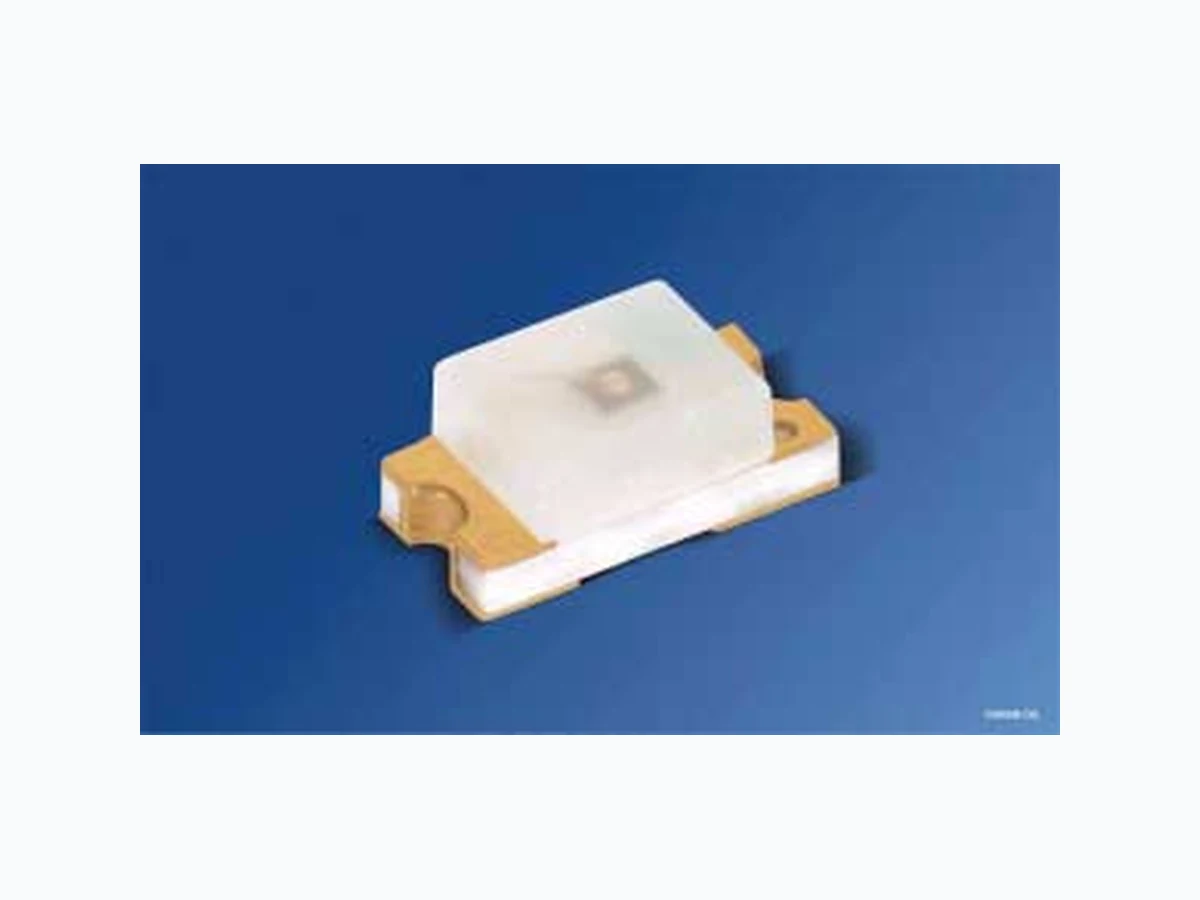
LSQ971 OSRAM
Document overview
- Manufacturer or author: Provided By www.digicamel.com(FREE DATASHEET DOWNLOAD SITE)
- PDF pages: 13
Technical content
Features
package: 0603, colorless diffused resin feature of the device: smallest package 1.6 mm x 0.8 mm x 0.8 mm wavelength: 628 nm (super-red), 606 nm (orange), 587 nm (yellow), 570 nm (green) viewing angle: extremely wide (160°) technology: GaP (green), GaAlP (super-red, orange, yellow) optical efficiency: 2.5 lm/W (green), 1.5 lm/W (super-red, orange, yellow) assembly methods: suitable for all SMT assembly methods soldering methods: IR reflow soldering preconditioning: acc. to JEDEC Level 2 taping: 8 mm tape with 4000/reel, ø180 mm ESD-withstand voltage: up to 2 kV acc. to JESD22-A114-D
Applications
indoor displays optical indicators flat backlighting (L CD, cellular phones, switches, displays) t o y s
LS Q971, LO Q971, LY Q971, LG Q971 Anm.: Die Standardlieferform von Serientypen beinhalt et alle Gruppen. Einzelne Helligkeitsgruppen sind nicht bestellbar. In einer Verpackungseinheit / Gurt ist immer nur eine Helligkeitsgruppe enthalten. Note: The standard shipping format for serial types includes all groups. Indivi dual brightness groups cannot be ordered. No packing unit / tape ever contains more than one brightness group. Bestellinformation
Ordering Information
Lichtstärke1) 2) Seite 13 Luminous Intensity 1) 2) page 13 IF = 20 mA IV (mcd) Bestellnummer Ordering Code min. typ. LS Q971 super-red 7.1 11 Q65110A4282 LO Q971 orange 4.5 9 Q65110A4285 LY Q971 yellow 2.8 6 Q62703Q4699 LG Q971 green 7.1 10 Q62702P5189
LS Q971, LO Q971, LY Q971, LG Q971 2007-10-08 3 Grenzwerte Maximum Ratings Bezeichnung Parameter Symbol Symbol Wert Value Einheit Unit LS LO LY LG Betriebstemperatur Operating temperature range Top – 30 … + 85 °C Lagertemperatur Storage temperature range Tstg – 40 … + 85 °C Sperrschichttemperatur Junction temperature Tj + 95 °C Durchlassstrom Forward current (TA=25°C) IF 25 25 20 25 mA Stoßstrom Surge current tp = 10 μs, D = 0.1, TA=25°C IFM 0.1 A Sperrspannung3) Seite 13 Reverse voltage3) page 13 (TA=25°C) VR 12 V Leistungsaufnahme Power consumption (TA=25°C) Ptot 65 65 50 65 mW Wärmewiderstand Thermal resistance Sperrschicht/Umgebung4) Seite 13 Junction/ambient4) page 13 Sperrschicht/Lötpad Junction/solder point Rth JA Rth JS 800 450 K/W K/W
LS Q971, LO Q971, LY Q971, LG Q971 Kennwerte Characteristics (TA = 25 °C) Bezeichnung Parameter Symbol Symbol Werte Values Einheit Unit LS LO LY LG Wellenlänge des emittierten Lichtes (typ.) Wavelength at peak emission IF = 20 mA λpeak 635 610 589 572 nm Dominantwellenlänge5) Seite 13 Dominant wavelength5) page 13 IF = 20 mA λdom 628 606 587 570 nm Spektrale Bandbreite (typ.) Spectral bandwidth IF = 20 mA Δλ 35 35 40 30 nm Abstrahlwinkel bei 50 % IV (Vollwinkel) (typ.) Viewing angle at 50 % IV 2ϕ 160 160 160 160 Grad deg. Durchlassspannung6) Seite 13 (typ.) Forward voltage6) page 13 (max.) IF = 20 mA VF VF 1.9 2.6 2.1 2.6 2.1 2.6 2.2 2.6 V V Sperrstrom (typ.) Reverse current (max.) VR = 12 V IR IR 0.02 100 0.02 100 0.02 100 0.02 100 μA μA Temperaturkoeffizient von λpeak (typ.) Temperature coefficient of λpeak IF = 20 mA; –10°C ≤ T ≤ 100°C TCλpeak 0.11 0.11 0.11 0.10 nm/K Temperaturkoeffizient von λdom (typ.) Temperature coefficient of λdom IF = 20 mA; –10°C ≤ T ≤ 100°C TCλdom 0.06 0.06 0.08 0.06 nm/K Temperaturkoeffizient von VF (typ.) Temperature coefficient of VF IF = 20 mA; –10°C ≤ T ≤ 100°C Optischer Wirkungsgrad (typ.) Optical efficiency IF = 20 mA ηopt 1.5 1.5 1.5 2.5 lm/W
LS Q971, LO Q971, LY Q971, LG Q971 2007-10-08 5 Relative spektrale Emission2) Seite 13 Relative Spectral Emission2) page 13 V(λ) = spektrale Augenempf indlichkeit / Standard eye response curve Irel = f (λ); TA = 25 °C; IF = 20 mA Abstrahlcharakteristik2) Seite 13 Radiation Characteristic2) page 13 Irel = f (ϕ); TA = 25 °C 400 relI 100 nm λ OHL02651 450 500 550 600 650 700 green yellow λV orange super red 0.2 0.4 1.0 0.8 0.6 ϕ 1.0 0.8 0.6 0.4 50˚ 60˚ 70˚ 80˚ 90˚ 100˚
LS Q971, LO Q971, LY Q971, LG Q971 2007-10-08 6 Durchlassstrom2) Seite 13 Forward Current2) page 13 IF = f (VF); TA = 25 °C Maximal zulässiger Durchlassstrom Max. Permissible Forward Current IF = f (TA) Relative Lichtstärke2) 7) Seite 13 Relative Luminous Intensity2) 7) page 13 IV/IV(20 mA) = f (IF); TA = 25 °C Relative Lichtstärke2) Seite 13 Relative Luminous Intensity2) page 13 IV/IV(25 °C) = f (TA); IF = 20 mA 10 -1 V OHL00636 mA 1.5 210 FI FV 2.0 2.5 3.0 3.5 10 1 10 0 F OHL02653 T I mA ˚C20 40 60 80 100 temp. ambientAT temp. solder pointTS ATT S green yellow orange super red V V (20 mA) 10 -1 0 10 10 12 10mA 10 -2 OHL00426110 I I 10 -1 10 0 FI T OHL02652 VI -20 0 20 40 60 ˚C 100 j 0.4 0.8 1.2 1.6 2IV (25 ˚C) yellow orange super red green
LS Q971, LO Q971, LY Q971, LG Q971 2007-10-08 7 Maßzeichnung8) Seite 13 Package Outlines8) page 13 Gewicht / Approx. weight: 1.4 mg Gurtung / Polarität und Lage8) Seite 13 Verpackungseinheit: 4 Rollen mit 4000/Rolle, 8 mm Gurt, ø180 mm Method of Taping / Polarity and Orientation8) page 13 Packing unit: 4 reels with 4000/reel, 8 mm tape, ø180 mm ø0.5 (ø0.020) 0.9 (0.035) mark Cathode 1.7 (0.067) 0.4 (0.016) 0.9 (0.035) Soldering terminal GEOY6989 0.7 (0.028) ø0.3 (ø0.012) 1.5 (0.059) 0.2 (0.008) 0.7 (0.028) Soldering terminal may flow in x, y direction 0.7 (0.028) 0.5 (0.020) 0.7 (0.028) 0.9 (0.035) Cathode mark C A OHAY1539 C A 4 (0.157) ±0.1 (0.004) ±0.05 (0.002)
LS Q971, LO Q971, LY Q971, LG Q971 Empfohlenes Lötpaddesign8) Seite 13 IR Reflow Löten Recommended Solder Pad8) page 13 IR Reflow Soldering Empfohlenes Lötpaddesign verwendbar für CHIPLED und Chipled - Bauform 0603 IR Reflow Löten8) 9) Seite 13 Recommended Solder Pad useable for CHIPLED and Chipled - Package 0603 IR Reflow Soldering8) 9) page 13 0.8 (0.031) 0.7 (0.028) OHAPY606 0.8 (0.031) 0.8 (0.031) OHPY0203 2.25 (0.089) 0.65 (0.026) 0.3 (0.012) 0.5 (0.020) 0.8 (0.031) 0.35 (0.014) 0.225 (0.009)
LS Q971, LO Q971, LY Q971, LG Q971 2007-10-08 9 Lötbedingungen Vorbehandlung nach JEDEC Level 2 Soldering Conditions Preconditioning acc. to JEDEC Level 2 IR-Reflow Lötprofil (nach CECC 00802) IR Reflow Soldering Profile (acc. to CECC 00802) IR-Reflow Lötprofil für bleifreies Löten (nach J-STD-020B) IR Reflow Soldering Profile for lead free soldering (acc. to J-STD-020B) OHLA0685 0:00 T t min 100 150 200 250 0:30 1:00 1:30 2:00 2:30 3:00 3:30 4:00 4:30 5:00 5:30 2-3 K/s 2-3 K/s T = 183 ˚C = 70 s t maxT = 245 ˚C OHLA0687 T t s 120 s max 100 150 200 250 300 Ramp Up 100 s max 50 100 150 200 250 300 Ramp Down
6 K/s (max)
3 K/s (max)
25 ˚C 30 s max 260 ˚C+0 ˚C -5 ˚C 245 ˚C ±5 ˚C 240 ˚C 255 ˚C 217 ˚C Maximum Solder Profile Recommended Solder Profile 235 ˚C-0 ˚C +5 ˚C Minimum Solder Profile 10 s min
LS Q971, LO Q971, LY Q971, LG Q971 Barcode-Produkt-Etikett (BPL) Barcode-Product-Label (BPL) Gurtverpackung Tape and Reel Tape dimensions in mm (inch) W P0 P1 P2 D0 E F 4 ± 0.1 (0.157 ± 0.004) 4 ± 0.1 (0.157 ± 0.004) 2 ± 0.05 (0.079 ± 0.002) 1.5 + 0.1 (0.059 + 0.004) 1.75 ± 0.1 (0.069 ± 0.004) 3.5 ± 0.05 (0.138 ± 0.002) Reel dimensions in mm (inch) A W Nmin W1 W2 max SampleOHA12043 X - X - X(G) GROUP: Lot Number(1T) LOT NO: (9D) D/C: Date Code (X) PROD NO: Product Code (6P) BATCH NO: Batch Number Lx xxxx Product Name RoHS Compliant Bin1: Bin Information Color 1 Bin2: Bin3: ML Temp ST
260 C RT
PACKVAR: Packing Type Product Quantity per Reel(Q)QTY: Semiconductors OSRAM Opto Wavelength Group Forward Voltage Group Brightness Group Bar Code Bar Code Bar Code W FE Direction of unreeling N A OHAY0324 Label Gurtvorlauf: Leader: Trailer: Gurtende: 13.0 Direction of unreeling ±0.25 160 mm 160 mm 400 mm 400 mm 8 + 0.3 – 0.1
LS Q971, LO Q971, LY Q971, LG Q971 Trockenverpackung und Materialien Dry Packing Process and Materials Anm.: Feuchteempfindliche Produkte sind verpackt in eine m Trockenbeutel zusammen mit einem Trockenmittel und einer Feuchteindikatorkarte Bezüglich Trockenverpackung finden Sie weitere Hinweise im Internet und in unserem Short Form Catalog im Kapitel “Gurtung und Verpackung” unter dem Punkt “Trockenverpackung ”. Hier sind Normenbezüge, unter anderem ein Auszug der JEDEC-Norm, enthalten. Note: Moisture-senisitve product is packed in a dr y bag containing desiccant and a humidity card. Regarding dry pack you will find furt her information in the internet and in the Short Form Catalog in chapter “Tape and Reel” under the topic “Dry Pack”. Here you will also find the normative references like JEDEC. Kartonverpackung und Materialien Transportation Packing and Materials OHA00539 OSRAM Moisture-sensitive label or print Barcode label Desiccant Humidity indicator Barcode label OSRAM Please check the HIC immidiately after bag opening. Discard if circles overrun. Avoid metal contact. WET Do not eat. Comparator check dot parts still adequately dry. examine units, if necessary examine units, if necessary 15% 10%bake units bake units If wet, change desiccant If wet, Humidity Indicator MIL-I-8835 If wet, M oisture Level 3 Floor tim e 168 Hours M oisture L evel 6 Floor tim e 6 Hours a) Hum idity Indicator C ard is > 10% w hen read a t 23 ˚C ± 5 ˚C , or reflow, vapor-p hase re flow, or equivalent p rocessing (peak package 2. After this bag is o pened, d evices th at will be subjected to infrare d 1. Shelf life in sealed bag: 24 m onths at < 4 0 ˚C and < 90% relative h um idity (RH). M oisture Level 5a at fa ctory conditions of (if b lank, seal date is identical w ith d ate code). a) M ounted w ithin b) Stored at body te m 3. Devices re quire baking, befo re m ounting, if: Bag seal date M oisture Level 1 M oisture Level 2 M oisture Level 2a4. If b aking is required, b) 2 a o r 2b is not m et. Date and tim e opened: re fere nce IPC/JEDEC J-STD-033 for bake p rocedure. Floor tim e see below If blank, see b ar code label Floor tim e > 1 Y ear Floor tim e 1 Year Floor tim e 4 W eeks10% RH. M oistu re Level 4 M oisture L evel 5 ˚C). OPTO SEMICONDUCTORS MOISTURE SENSITIVE This bag contains CAUTION Floor tim e 72 Hours Floor tim e 48 H ours Floor tim e 24 Hours 30 ˚C/60% R LEVEL If blank, see bar code label OHA02624 PACKVAR:R077 Additional TE XT P-1+Q-1 Multi TOPLED Muster OSRAM Opto Semiconductors (6P) BATCH NO: (X) PROD NO: 10 (9D) D/C:11 (1T) LOT NO 210021998 123GH1234 0 245 (Q)QTY: 2000 0144 (G) GROUP: 260 C RT
240 C R3 220 C R
Bin3:Bin2: Q-1-20Bin1: P-1-20 LSY T676 22a Temp S T R18 DEMY
LS Q971, LO Q971, LY Q971, LG Q971 Attention please! The information describes the type of component and shall not be considered as assured characteristics. Terms of delivery and rights to change design reserv ed. Due to technical requirements components may contain dangerous substances. For information on the types in question please contact our Sales Organization. If printed or downloaded, please find the latest version in the Internet. Packing Please use the recycling operators known to you. We can also help you – get in touch with your nearest sales office. By agreement we will take packing material back, if it is sorted. You must bear the costs of tr ansport. For packing material that is returned to us unsorted or which we are not obliged to accept, we shall have to invoice you for any costs incurred. Components used in life-support devices or system s must be expressly authorized for such purpose! Critical components10) page 13 may only be used in life-support devices or systems 11) page 13 with the express written approval of OSRAM OS. Revision History: 2007-10-08 Previous Version: 2005-06-30 Page Subjects (major changes since last revision) Date of change 9 recommended solder pad 4 forward voltage 3 pad size from 16 mm2 to 5 mm2 11 annotations 2002-07-23 3, 4 value (reverse voltage from 5 V to 12 V) 2002-09-18 2 ordering code 2002-09-19 3 ambient temperature 2003-09-04 all new template 2004-03-22 all RoHS compliant 2004-08-12
1 ESD-withstand voltage 2004-08-30
10 Product Label acc. to OS-IN-2005-015 2005-05-18 all new colors: super-red, orange 2005-06-30 2 new brightness grouping of LY Q971 - new Q-number 2007-10-08
LS Q971, LO Q971, LY Q971, LG Q971 2007-10-08 13 Fußnoten: 1) Helligkeitswerte werden mit einer Stromeinprägedauer von 25 ms und einer Genauigkeit von ± 11% ermittelt. 2) Wegen der besonderen Prozessbedingungen bei der Herstellung von LED können typische oder abgeleitete technische Parameter nur aufgrund statistischer Werte wiedergegeben werden. Diese stimmen nicht notwendigerweise mit den Werten jedes einzelnen Produktes überein, dessen Werte sich von typischen und abgeleiteten Werten oder typischen Kennlinien unterscheiden können. Falls erforderlich, z.B. aufgrund technischer Verbesserungen, werden diese typischen Werte ohne weitere Ankündigung geändert. 3) Die LED kann kurzzeitig in Sperrichtung betrieben werden. 4) Montage auf PC-Board FR 4 (Padgröße ≥ 5 mm2) 5) Wellenlängen werden mit einer Stromeinprägedauer von 25 ms und einer Genauigkeit von ±1 nm ermittelt. 6) Spannungswerte werden mit einer Stromeinprägedauer von 1 ms und einer Genauigkeit von ±0,1 V ermittelt. 7) Im gestrichelten Bereich der Kennlinien muss mit erhöhten Helligkeitsunterschieden zwischen Leuchtdioden innerhalb ei ner Verpackungseinheit gerechnet werden. 8) Maße werden wie folgt angegeben: mm (inch) 9) Empfohlene Lötpastendicke: 120 µm 10) Ein kritisches Bauteil ist ein Bauteil, das in lebenserhaltenden Apparaten oder Systemen eingesetzt wird und dessen Defekt voraussichtlich zu einer Fehlfunktion dieses lebenserhaltenden Apparates oder Systems führen wird oder die Sicherheit oder Effektivit ät dieses Apparates oder Systems beeinträchtigt. 11) Lebenserhaltende Apparate oder Systeme sind für (a) die Implantierung in den menschlichen Körper oder (b) für die Lebenserhaltung bestimmt. Falls sie versagen, kann davon ausgegangen werden, dass die Gesundheit und das Leben des Patienten in Gefahr ist. Published by OSRAM Opto Semiconductors GmbH Wernerwerkstrasse 2, D-93049 Regensburg www.osram-os.com © All Rights Reserved. Remarks: 1) Brightness groups are test ed at a current pulse duration of 25 ms and a tolerance of ± 11%. 2) Due to the special conditions of the manufacturing processes of LED, the ty pical data or calculated correlations of technical pa rameters can only reflect statistical figures. These do not necessarily correspond to the actual parameters of each single product, which could differ from the typical data and calculated correlations or the typical characteristic line. If requested, e.g. because of technical improvements, these typ. data will be changed without any further notice. 3) Driving the LED in reverse direction is suitable for short term application. 4) Mounted on PC board FR 4 (pad size ≥ 5 mm2) 5) Wavelengths are tested at a current pulse duration of ms and a tolerance of ±1 nm. 6) Forward voltages are tested at a current pulse duration of 1 ms and a tolerance of ±0.1 V. 7) In the range where the line of the graph is broken, you must expect higher bright ness differences between single LEDs within one packing unit. 8) Dimensions are specified as follows: mm (inch). 9) Recommended thickness of solder paste: 120 µm 10) A critical component is a component used in a life-support device or system whose failure can reasonably be expected to cause the failure of that life-support device or system, or to affect its safety or the effectiveness of that device or system. 11) Life support devices or systems are intended (a) to be implanted in the human body, or (b) to support and/or maintain and sustain human life. If they fail, it is reasonable to assume that the health and the life of the user may be endangered.