
LMD10P100 LEIDITECH
Document overview
- Manufacturer or author: Provided By www.digicamel.com(FREE DATASHEET DOWNLOAD SITE)
- PDF pages: 6
Technical content
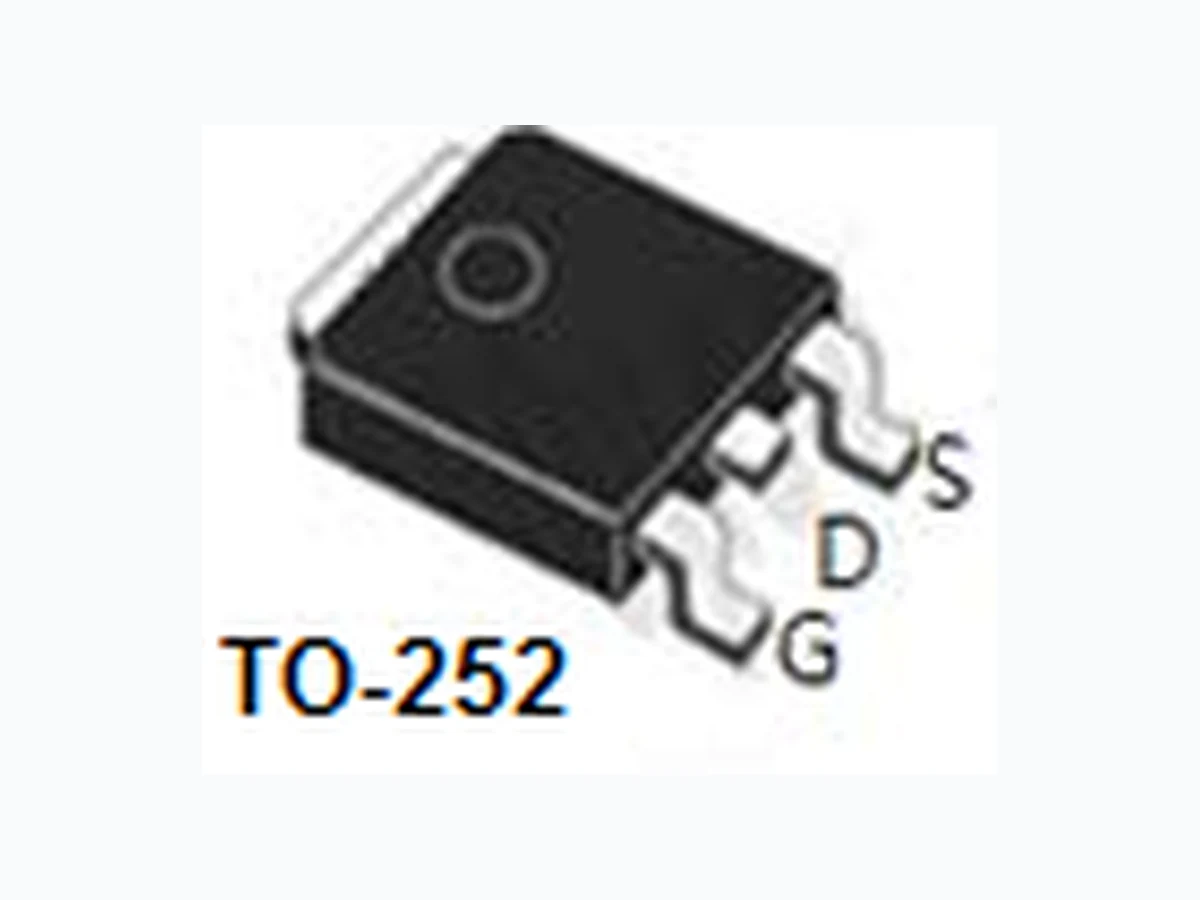
Device Marking and Package Information Device Package Marking LMD10P100 TO-252
FEATURES
Super Low Gate Charge 100% EAS Guaranteed RoHS compliant Green Device Available Excellent CdV/dt effect decline Advanced high cell density Trench technology
APPLICATIONS
Switch Mode Power Supply (SMPS) Uninterruptible Power Supply (UPS) Power Factor Correction (PFC) Absolute Maximum Ratings at Tj= 25ºC unless otherwise noted Parameter Symbol Value Unit Drain-Source Voltage (VGS = 0V) VDSS -100 V Continuous Drain Current TC = 25ºC (note1) ID -30 A Continuous Drain Current TC = 100ºC (note1) -21 A Pulsed Drain Current (note2) IDM -52 A Gate Source Voltage VGSS ±20 V Single Pulse Avalanche Energy (note3) EAS 110 mJ Power Dissipation TC = 25ºC (note4) PD 69.3 W Operating Junction and Storage Temperature Range TJ, Tstg -55~+150 ºC Thermal Characteristics Parameter Symbol Value Unit Thermal Resistance, Junction-Case (note1) RθJC 1.3 K/W Thermal Resistance, Junction-to-Ambient (note1) RθJA 62 LMD10100 P-Channel Enhancement Mode Power MOSFET Rev : www.leiditech.com 01.06.2018
Electrical Characteristics Tj= 25ºC unless otherwise specified Parameter Symbol Test Conditions Value Unit Min. Typ. Max. Static Drain-Source Breakdown Voltage V(BR)DSS VGS = 0V, ID = 250µ A -100 -- -- V Zero Gate Voltage Drain Current IDSS VDS = -100V, VGS = 0V, TJ = 25ºC -- -- -50 uA VDS = -100V, VGS = 0V, TJ = 55ºC -- -- -60 uA Gate-Source Leakage IGSS VGS = ±20V -- -- ±100 nA Gate-Source Threshold Voltage VGS(th) VDS = VGS, ID = 250µ A -1.2 -- -2.5 V Drain-Source On-Resistance (note2) RDS(on) VGS = -10V, ID = -12A -- 80 100 mΩ VGS = -4.5V, ID = -9A -- 88 115 mΩ Dynamic Input Capacitance Ciss VGS = 0V, VDS = -20V, f = 1.0MHz -- 3029 -- pFOutput Capacitance Coss -- 129 -- Reverse Transfer Capacitance Crss -- 76 -- Total Gate Charge (4.5V) Qg VDs = -50V, ID = -20A, VGS = -10V -- 44.5 -- nCGate-Source Charge Qgs -- 9.13 -- Gate-Drain Charge Qgd -- 5.93 -- Turn-on Delay Time td(on) VDS = -50V, ID = -10A, VGS = -10V,RG = 3.3Ω -- 12 -- ns Turn-on Rise Time tr -- 27.4 -- Turn-off Delay Time td(off) -- 79 -- Turn-off Fall Time tf -- 53.6 -- Body Diode Characteristics Continuous Body Diode Current IS TC = 25 º C -- -- -30 A Pulsed Diode Forward Current ISM -- -- -52 Body Diode Voltage VSD TJ = 25º C, ISD = -1A, VGS = 0V -- -- 1.2 V Reverse Recovery Time trr IF = -14A diF/dt = 100A/μs -- 38.7 -- ns Reverse Recovery Charge Qrr -- 22.4 -- nC Notes 1. The data tested by surface mounted on a 1 inch2 FR-4 board with 2OZ copper. 2. The data tested by pulsed , pulse width≦300us , duty cycle≦2% 3. The EAS data shows Max. rating . The test condition is VDD =25V,VGS =10V,L=0.85mH 4. The power dissipation is limited by 175℃junction temperature 5. The data is theoretically the same as ID and IDM , in real applications , should be limited by total power dissipation. LMD10100 Rev : www.leiditech.com 01.06.2018
Typical Characteristics TJ = 25ºC, unless otherwise noted Fig.1 Typical Output Characteristics Fig.2 On-Resistance vs. G-S Voltage Fig.5 Normalized VGS(th) vs. TJ Fig.6 Normalized RDSON vs. TJ Fig.3 Forward Characteristics of Reverse Diode Fig.4 Gate-Charge Characteristics LMD10100 Rev : www.leiditech.com 01.06.2018
Typical Characteristics TJ = 25ºC, unless otherwise noted Fig.7 Capacitance Fig.8 Safe Operating Area Fig.9 Normalized Maximum Transient Thermal Impedance LMD10100 Rev : www.leiditech.com 01.06.2018
Figure A:Gate Charge Test Circuit and Waveform Figure B:Resistive Switching Test Circuit and Waveform Figure C:Unclamped Inductive Switching Test Circuit and Waveform LMD10100 Rev : www.leiditech.com 01.06.2018
Shanghai Leiditech Electronic Co.,Ltd Email: sale1@leiditech.com Tel : +86- 021 50828806 Fax : +86- 021 50477059 Rev : www.leiditech.com 01.06.2018