
LM8S9N04 LEIDITECH
Document overview
- Manufacturer or author: Provided By www.digicamel.com(FREE DATASHEET DOWNLOAD SITE)
- PDF pages: 6
Technical content
Description
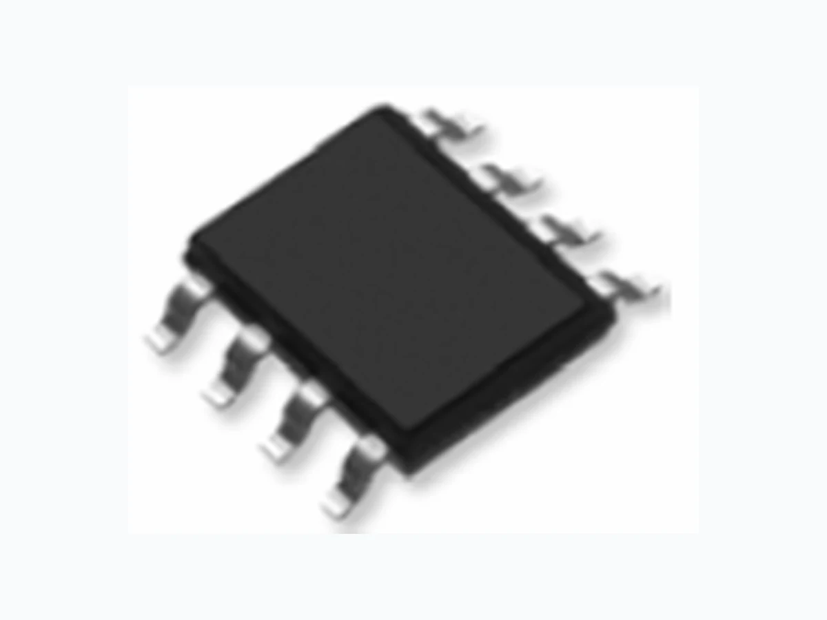
The LM8S9N04 uses advanced trench technology to provide excellent R DS(ON) and low gate charge . The complementary MOSFETs may be used to form a level shifted high side switch, and for a host of other applications. General Features
- N-Channel V DS =40V,I D =9A R DS(ON) < 16mΩ @ V GS =10V R DS(ON) < 24mΩ @ V GS =4.5V
- High power and current handing capability
- Lead free product is acquired
- Surface mount package Schematic diagram Marking and pin assignment SOP-8 top view Package Marking and Ordering Information Device Marking Device Device Package Reel Size Tape width Quantity NCE4009S LM8S9N04 SOP-8 Ø330mm 12mm 4000units Absolute Maximum Ratings (T C =25℃unless otherwise noted) Parameter Symbol Limit Unit Drain-Source Voltage V DS 40 V Gate-Source Voltage V GS ±20 V Drain Current-Continuous I D 9 A Drain Current-Continuous(T C =100℃) I D (100℃) 6.4 A Pulsed Drain Current I DM 40 A Maximum Power Dissipation P D 2 W Operating Junction and Storage Temperature Range T J STG -55 To 150 ℃ Thermal Characteristic Thermal Resistance,Junction-to-Ambient (Note 2) R θJA 62.5 /W℃ Enhancement Mode Power MOSFET Rev : www.leiditech.com 01.06.2014 N-Channel
A =25℃unless otherwise noted) Parameter Symbol Condition Min Typ Max Unit Off Characteristics Drain-Source Breakdown Voltage BV DSS V GS =0V I D =250μA 40 - - V Zero Gate Voltage Drain Current I DSS V DS =40V,V GS =0V - - 1 μA Gate-Body Leakage Current I GSS V GS =±20V,V DS =0V - - ±100 nA On Characteristics (Note 3) Gate Threshold Voltage V GS(th) V DS GS D =250μA 1 1.5 2.0 V V GS =10V, I D =8A - 12.9 16 m Ω Drain-Source On-State Resistance R DS(ON) V GS =4.5V, I D =4A - 18.9 24 m Ω Forward Transconductance g FS V DS =5V,I D =8A 33 - - S Dynamic Characteristics (Note4) Input Capacitance C lss - 415 - PF Output Capacitance C oss - 112 - PF Reverse Transfer Capacitance C rss V DS =20V,V GS =0V, F=1.0MHz - 11 - PF Switching Characteristics (Note 4) Turn-on Delay Time t d(on) - 4 - nS Turn-on Rise Time t r - 3 - nS Turn-Off Delay Time t d(off) - 15 - nS Turn-Off Fall Time t f V DD =20V, R L =2.5Ω V GS =10V,R GEN =3Ω - 2 - nS Total Gate Charge Q g - 12 - nC Gate-Source Charge Q gs - 3.2 - nC Gate-Drain Charge Q gd V DS =20V,I D =8A, V GS =10V - 3.1 - nC Drain-Source Diode Characteristics Diode Forward Voltage (Note 3) V SD V GS =0V,I S =9A - 0.8 1.2 V Rev : www.leiditech.com 01.06.2014 LM8S9N04
Square Wave Pluse Duration(sec) Figure 13 Normalized Maximum Transient Thermal Impedance r(t),Normalized Effective Transient Thermal Im p edance Rev : www.leiditech.com 01.06.2014 LM8S9N04
Dimensions In Millimeters Dimensions In Inches Symbol Min. Max. Min. Max. A 1.350 1.750 0.053 0.069 A1 0.100 0.250 0.004 0.010 A2 1.350 1.550 0.053 0.061 b 0.330 0.510 0.013 0.020 c 0.170 0.250 0.006 0.010 D 4.700 5.100 0.185 0.200 E 3.800 4.000 0.150 0.157 E1 5.800 6.200 0.228 0.244 e 1.270(BSC) 0.050(BSC) L 0.400 1.270 0.016 0.050 θ 0° 8 ° 0 ° 8 ° Shanghai Leiditech Electronic Co.,Ltd Email: sale1@leiditech.com Tel : +86- 021 50828806 Fax : +86- 021 50477059 Rev : www.leiditech.com 01.06.2014 LM8S9N04